Introduction
PCB panelization is the practice of grouping multiple boards into a single manufacturing panel. This approach improves production efficiency, reduces handling time, and lowers overall costs during assembly.
Early panelization helps prevent misalignment, depaneling stress, and edge component damage. A good array layout also ensures compatibility with automated processes such as SMT placement, wave soldering, and optical inspection.
This guide explains V-scoring vs tab routing, panel frame design, fiducial and tooling hole placement, and layout optimization for assembly.
Choosing V‑Scoring or Tab‑Routing
In PCB panelization, how you separate individual boards matters. The two most common methods are V‑scoring and Tab‑routing.
V‑Scoring
V‑scoring creates shallow V‑shaped grooves on the top and bottom surfaces of the board. Boards are snapped apart after assembly.
Use V‑scoring for rectangular boards without edge components to maximize panel density and reduce cost.
Pros:
High material utilization
Fast and cost-effective
Simple panel design
Cons:
Only works with straight edges
Edge components can be damaged during breaking
May introduce mechanical stress
Tab‑Routing
Tab‑routing connects boards using small tabs, sometimes with perforations (mouse bites). Tabs are broken manually or with tools after assembly
Use Tab‑routing for boards with irregular shapes, edge‑mounted components, or when lower depaneling stress is required.
Pros:
Supports complex shapes
Safer for edge-mounted components
Cleaner edges with CNC routing
Cons:
More spacing required between boards
Slightly higher manufacturing cost
Tabs may leave rough edges if not routed
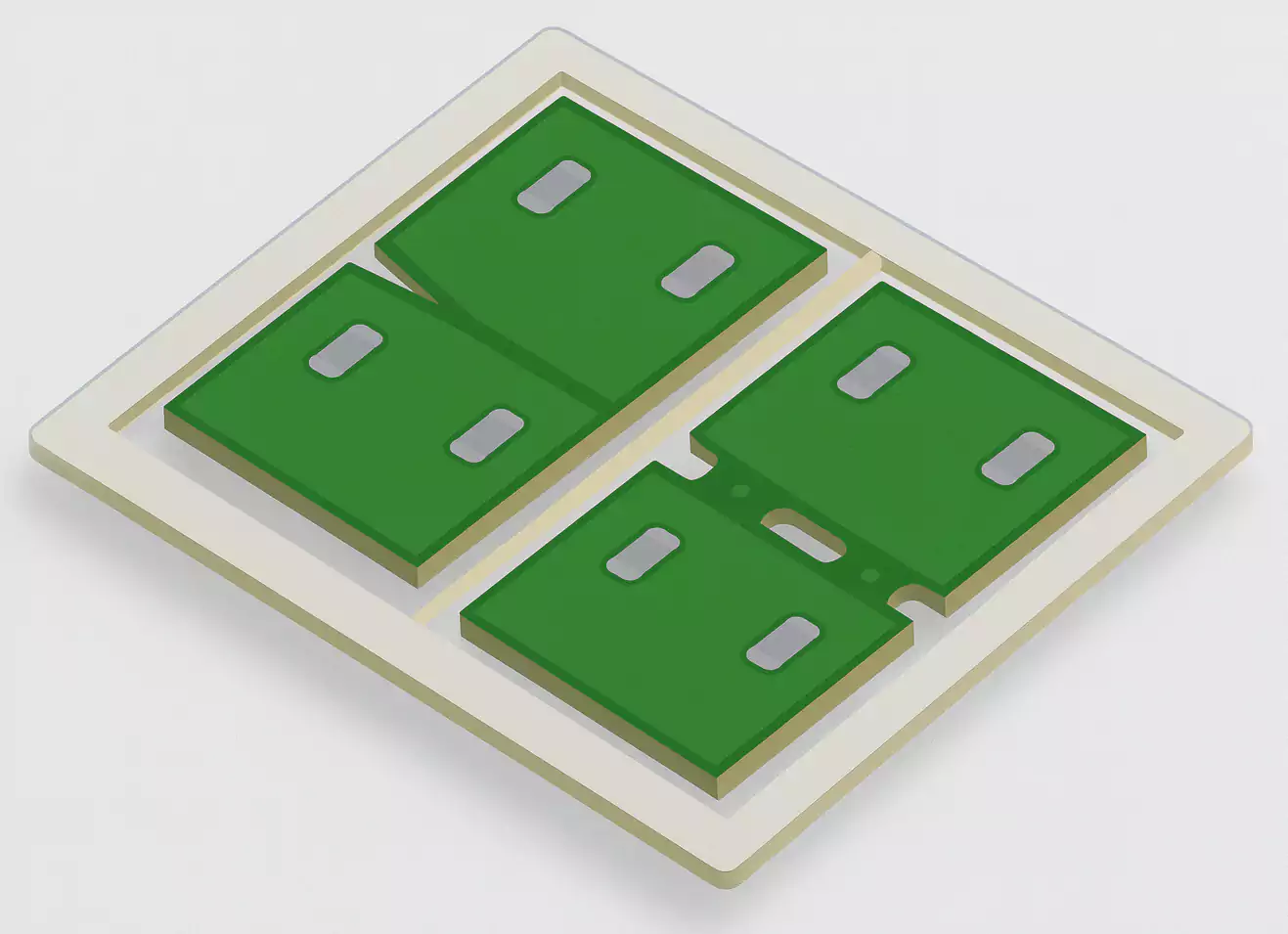
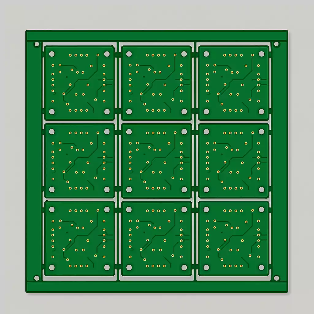
Array Layout Planning: Efficient Arrangement for Manufacturing
1. Board Orientation
All boards in the array should face the same direction to streamline pick-and-place, inspection, and routing. Consistent orientation reduces machine programming complexity and assembly errors.
2. Spacing Between Boards
Spacing depends on the depaneling method:
V-scoring: allows minimal spacing (0–0.5 mm)
Tab-routing: requires more space (1.0–2.0 mm) to accommodate router paths and tab bridges
3. Panel Size and Utilization
Standard panel size is typically 18" x 24", with a usable area around 16" x 22" after edge clearance.
To optimize:
Fit as many boards as possible within the usable area
Maintain a 5–10 mm border for tooling holes and fiducials
Use symmetric layouts to prevent warping during reflow
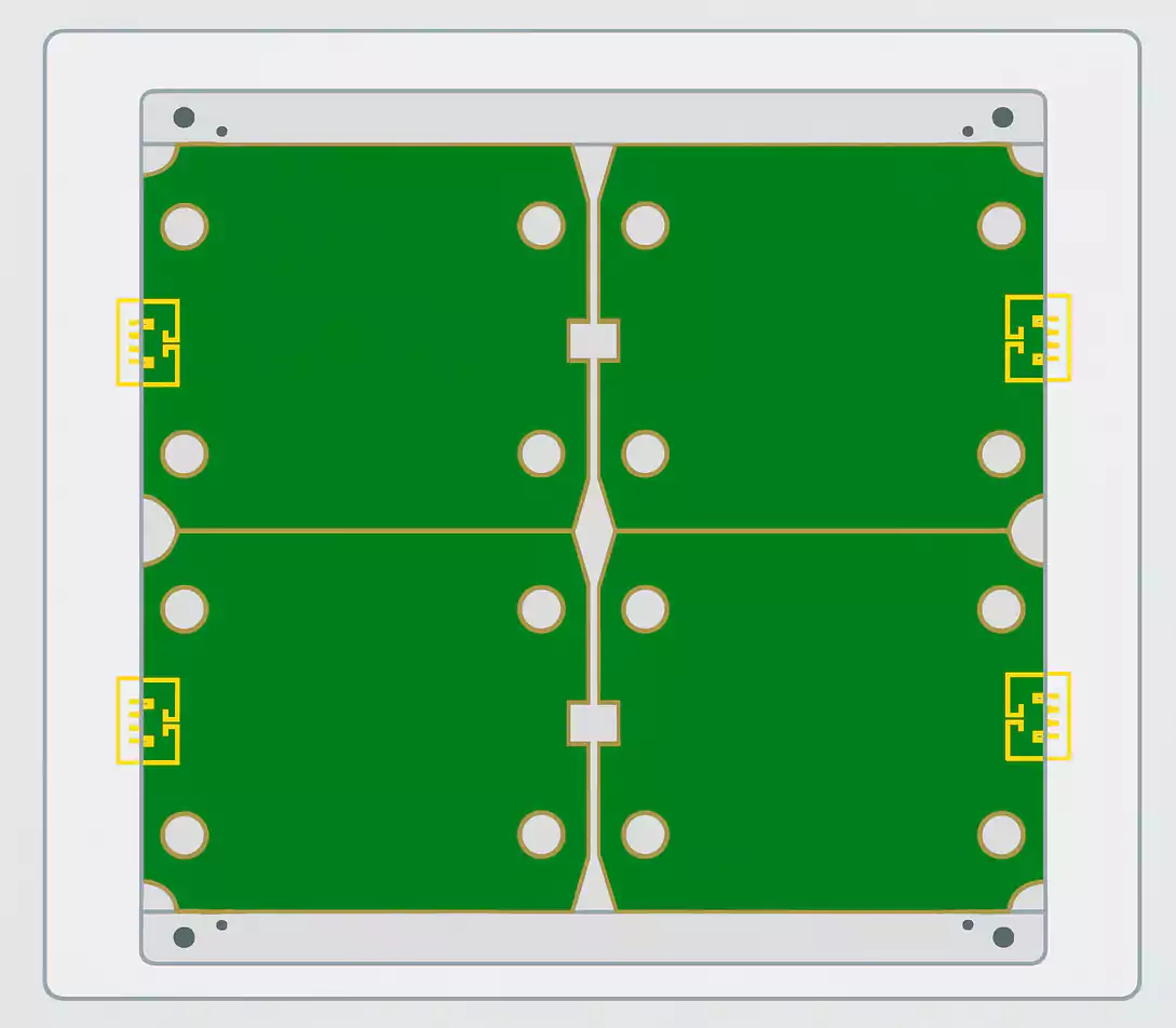
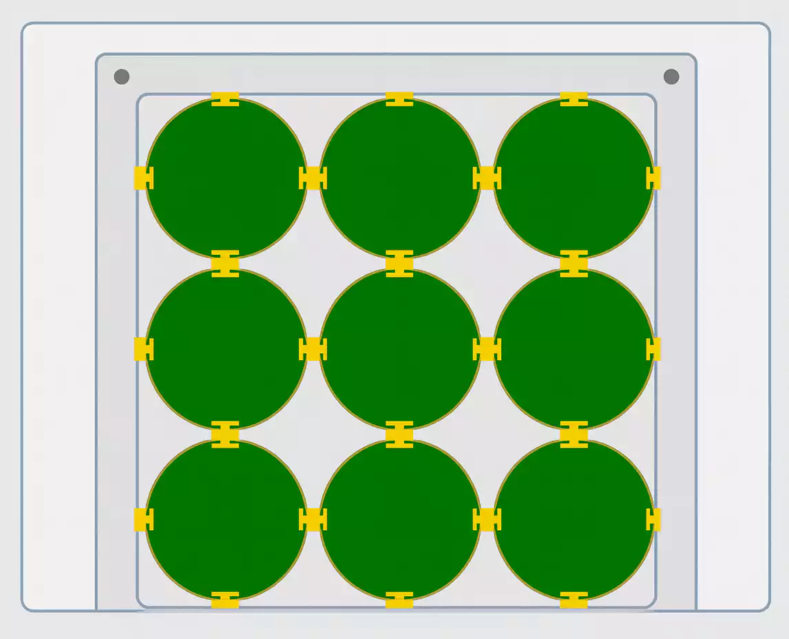
Edge Rails and Tooling Features in PCB Panelization
Edge rails and tooling holes are essential mechanical features in a panelized PCB layout. They improve handling, ensure machine compatibility, and help maintain structural integrity during assembly.
Edge Rails (Breakaway Rails)
Edge rails are non-functional margins added to the panel's perimeter. They allow automated equipment—such as SMT conveyors and depaneling tools—to grip, align, and process the panel safely.
Tooling Holes
Tooling holes are used for precise alignment during stencil printing, pick-and-place, and testing.
Fiducial Points and Pick-and-Place Alignment
Fiducial markers are essential reference points used by automated optical systems—particularly pick-and-place machines and AOI (Automated Optical Inspection)—to accurately align the PCB during assembly.
What Is a Fiducial Point?
A fiducial point is a copper pad, usually circular and uncovered (no solder mask), that acts as a global or local alignment marker. Vision systems detect the position of these fiducials to calculate rotation and offset, ensuring precise component placement.
Global vs. Local Fiducials
There are two main types of fiducial markers in PCB panelization:
Global Fiducials: Placed on the panel frame (rails), typically three points forming an L-shape or triangle. These help align the entire array for the first pass of SMT.
Local Fiducials: Placed on individual PCBs within the array, especially useful for boards with fine-pitch components like BGAs or QFNs. They compensate for any local warping or misregistration.
Fiducial Points in Panelized PCBs
When designing panelized arrays, it’s recommended to:
Add three global fiducials on the tooling frame (top-left, top-right, and bottom-left corners).
Include local fiducials on each sub-board if component placement requires higher precision.
Ensure that fiducials are not placed on V-score lines, break-away tabs, or regions affected by routing stress.
Cost and Manufacturing Optimization Tips
Use Standard Panel Sizes
Stick to your manufacturer’s standard panel sizes—commonly 18"×24" or 16"×22".
Board Count per Panel
Fit as many boards as possible into the panel without compromising spacing or depaneling requirements.
Choose the Right Depaneling Method
V-scoring is faster and cheaper but only works for rectangular boards without edge components.
Tab-routing suits complex shapes and edge-mounted parts but takes longer and may need post-processing.
Keep Copper Balanced
Unbalanced copper can cause warping, especially during reflow. To avoid this:
Distribute copper evenly on both layers
Avoid large solid pours on one side only
Keep component layout symmetrical
Conclusion
PCB panelization isn’t just about manufacturing—it’s a key design step that impacts cost, efficiency, and assembly quality. Planning it early helps reduce waste and streamline production.

Choosing the right depaneling method, setting proper spacing, adding fiducials, and reserving edge rails should be part of your standard design flow.
Treat panelization as an integral part of your DFM strategy—not a post-design patch. A well-planned panel saves time, lowers costs, and helps your product scale with confidence.