Introduction
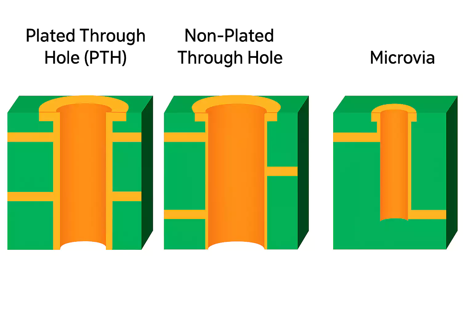
Printed Circuit Boards (PCBs) are the backbone of all modern electronic devices, and at the heart of every PCB lies a critical process that connects multiple layers and components—drilling and plated-through holes (PTH). Whether it’s for signal transmission, component mounting, or inter-layer connectivity, drilled holes and their subsequent metallization play an essential role in ensuring a PCB’s functionality and reliability.
With the growing demand for high-density interconnects (HDI), miniaturization, and complex multilayer stackups, PCB drilling methods have evolved to include not just traditional mechanical drilling, but also laser drilling for microvias and blind/buried vias. Alongside, hole wall metallization—typically achieved through electroless and electrolytic copper plating—must meet increasingly tight tolerance and reliability standards.
PCB Drilling Methods: Mechanical vs. Laser Drilling
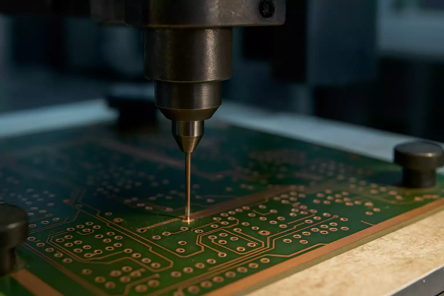
Drilling is a fundamental step in printed circuit board (PCB) fabrication, serving as the foundation for plated-through holes (PTH), vias, and component mounting. Two primary technologies dominate the PCB drilling process: mechanical drilling and laser drilling. Each method has specific applications, advantages, limitations, and manufacturing constraints that must be understood to ensure optimal board performance and manufacturability.
1.Mechanical Drilling
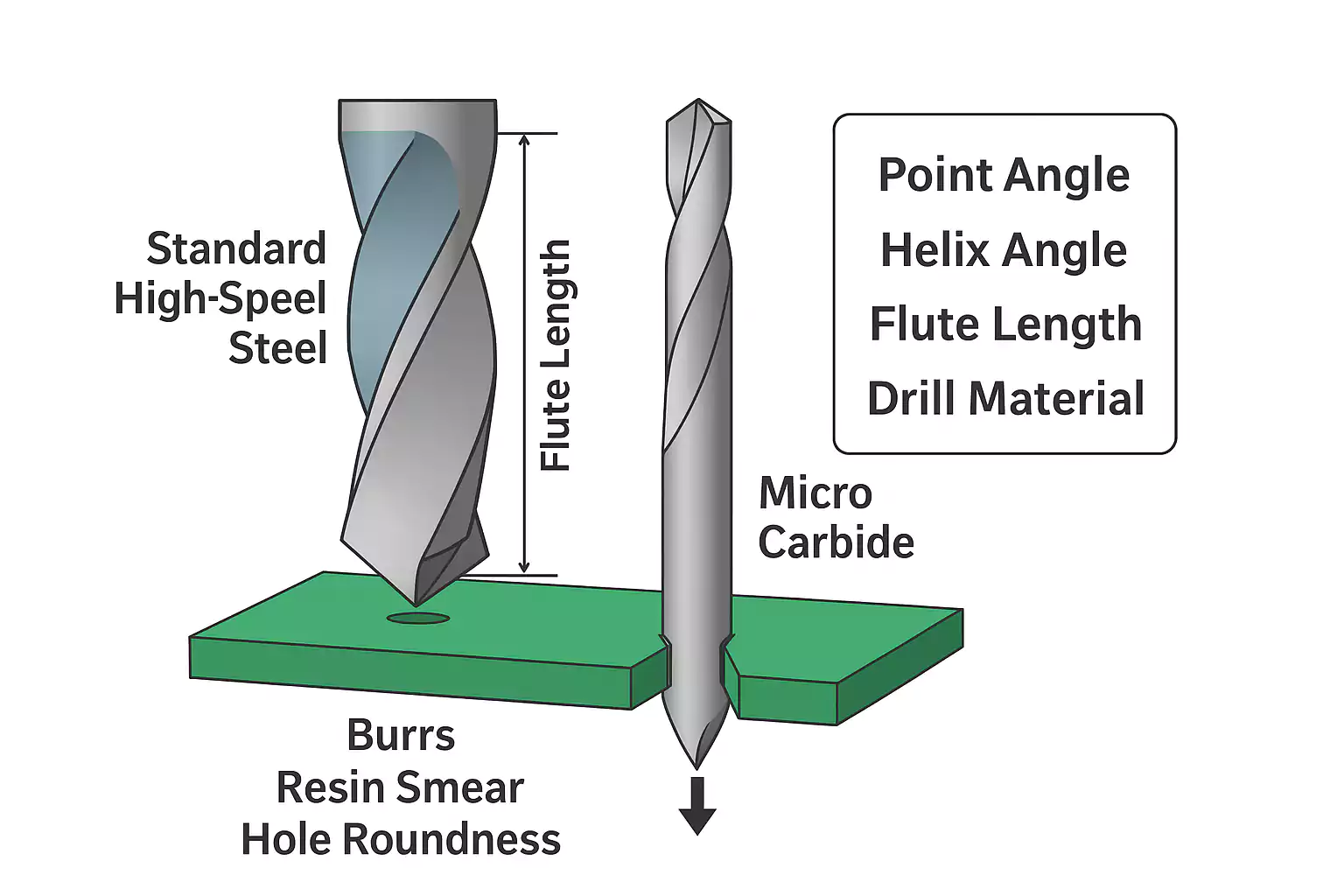
Mechanical drilling is the most common method used to create holes in PCBs. It involves high-speed spindles (typically 150,000–300,000 RPM) and micro-diameter drill bits made from solid carbide or tungsten steel to penetrate laminated PCB substrates.
Key Features:
- Hole Size Range: Typically from 0.15 mm (6 mils) up to several millimeters
- Precision: Suitable for through-hole vias, component mounting holes, and larger plated vias
- Cost-Effective: Lower cost per hole compared to laser when drilling standard via sizes
- High Throughput: Multiple heads can drill simultaneously for mass production
Typical Mechanical Drilling Process:
- Drill file generation (NC drill data from PCB layout)
- Tool path optimization
- Drilling using CNC machines
- Deburring and desmearing post-process steps
Limitations:
- Minimum Drill Size: Limited to around 0.15 mm due to drill bit strength and breakage risk
- Aspect Ratio Constraints: Typically up to 10:1 (board thickness to hole diameter); going beyond increases the risk of poor plating coverage
- Tool Wear: Drill bits degrade with use, impacting dimensional accuracy and requiring constant calibration
- Drill-to-Copper Clearance: Needs to be considered to prevent breakout or damage to inner layers
2.Laser Drilling
Laser drilling is the preferred technique for creating microvias, especially in high-density interconnect (HDI) PCBs. It uses focused laser beams to ablate material and form precise holes without mechanical contact.
Key Features:
- Hole Size Range: As small as 0.05 mm (2 mils)
- Non-Contact Process: Eliminates mechanical stress on the board
- Ideal for Blind/Buried Vias: Excellent for layer-to-layer interconnections in HDI boards
- Superior Accuracy: High-precision drilling for dense circuit layouts
Types of Lasers Used:
- UV Laser (355 nm): Best suited for materials like FR-4, polyimide, and resin-based substrates
- CO₂ Laser (10.6 µm): Used for softer materials or drilling prepreg and coverlay
- Nd:YAG Laser: Less common now, replaced by UV lasers in many facilities
Limitations:
- Limited Aspect Ratio: Microvias are typically drilled with a depth-to-diameter ratio ≤ 1:1
- Material Compatibility: Not all PCB materials respond well to laser energy; can cause carbonization or poor hole definition
- Higher Cost: Equipment and operational costs are higher, especially for small production runs
- Through-Hole Incompatibility: Not suitable for deep or large-diameter plated through-holes
Mechanical vs. Laser Drilling: Comparison Table
| Feature | Mechanical Drilling | Laser Drilling |
|---|---|---|
| Hole Size Range | 0.15 mm – 6 mm+ | 0.05 mm – 0.3 mm (microvias) |
| Speed | High | Moderate (single hole per shot) |
| Minimum Annular Ring | Larger required | Very small possible |
| Aspect Ratio | Up to 10:1 | Typically 1:1 |
| Cost per Hole | Lower | Higher |
| Use Case | PTH, via, component holes | Microvias, HDI, blind vias |
| Material Stress | Moderate (mechanical) | Minimal (non-contact) |
Plated‑Through Hole (PTH) Metallization Process
Plated-through holes (PTH) are a critical aspect of multilayer PCB manufacturing, enabling vertical interconnect access between layers. Once the holes are drilled—either mechanically or via laser—their internal walls must be properly metallized to create reliable electrical connectivity and ensure long-term performance. Below is a step-by-step breakdown of the metallization process and key considerations for optimal quality.
1. Pre-Treatment and Cleaning
Before any plating can occur, the freshly drilled holes must be cleaned and prepared to ensure adhesion and electrical continuity:
- Deburring & Desmearing: Mechanical drilling often leaves behind burrs and resin smear on the hole walls. Chemical desmear processes (typically using potassium permanganate or plasma) remove these residues and roughen the hole wall to enhance copper adhesion.
- Etchback (optional): In high-reliability applications (IPC Class 3), etchback is used to expose inner layer copper cleanly, improving the connection between layers.
2. Hole Activation
Since the base material (FR-4 or other laminates) is non-conductive, the hole walls must be seeded with a catalyst to allow copper deposition:
- Catalyzation: A palladium-based solution is commonly used to deposit a thin conductive layer or activate the surface for electroless copper plating.
- Acceleration Step: Removes excess catalyst and ensures only active sites remain for uniform deposition.
3. Electroless Copper Deposition
Electroless copper (also called chemical copper) forms the initial conductive layer on the hole wall, connecting all copper layers and creating a continuous electrical path.
- Thickness: Typically between 0.5 to 1.0 μm (20–40 μin)
- Key Properties: Provides excellent coverage even in high aspect ratio holes, ensuring conductivity before electrolytic plating.
4. Electrolytic Copper Plating
Once electroless copper is deposited, the panel is placed in an electroplating bath to build up copper thickness to IPC or design requirements.
- Plating Thickness:
- Minimum: IPC-6012 Class 2 requires ≥ 20 μm (≈ 0.8 mil) of copper plating inside the hole barrel.
- Best Practice: 25–30 μm (≈ 1.0–1.2 mil) for added reliability.
- Throwing Power: Indicates how uniformly copper is plated inside deep or small-diameter holes. It’s affected by current density, solution agitation, and aspect ratio.
- Aspect Ratio Consideration: The higher the aspect ratio (hole depth vs diameter), the harder it is to achieve uniform plating.
5. Via Filling and Plugging (Optional for HDI & High-Reliability Boards)
For microvias, via-in-pad designs, or boards requiring flat surfaces, the holes may be filled with:
- Conductive Fill (e.g., electroplated copper): Supports current conduction and planarization.
- Non-Conductive Fill (e.g., epoxy): Used for mechanical support or capping before BGA or pad finishes.
Key Factors for Quality Hole Plating
| Factor | Impact |
|---|---|
| Cleaning & Desmear | Ensures adhesion and removes drilling residues |
| Catalyst Coverage | Uniform activation prevents skip plating |
| Electroless Copper Quality | Essential for hole integrity under stress |
| Current Density Control | Affects thickness uniformity inside holes |
| Plating Time & Temperature | Must be carefully controlled to avoid thin walls or nodular growth |
| Agitation & Filtration | Prevents particle accumulation and ensures even distribution |
Factors Affecting PCB Hole Wall Quality
The quality of plated-through holes (PTH) plays a critical role in the mechanical integrity, electrical reliability, and overall performance of a printed circuit board. Poor hole wall quality can lead to issues like conductivity failure, delamination, or even complete board rejection. Several interrelated factors impact hole wall quality during the PCB drilling and metallization processes. Below, we explore the most significant ones and how to manage them effectively.
1. Aspect Ratio and Hole Geometry
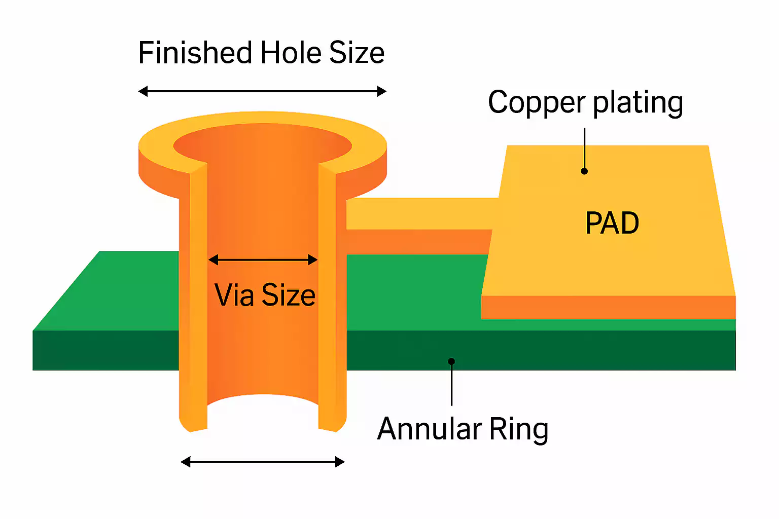
The aspect ratio—defined as the ratio of board thickness to the drilled hole diameter—directly influences plating uniformity inside the hole. Higher aspect ratios make it more difficult for plating solution to reach the center of the barrel, resulting in thin or non-uniform copper deposits. For mechanical drilling, most board shops recommend an aspect ratio below 10:1, though high-reliability applications may require even stricter limits.
Additionally, hole roundness and diameter consistency are vital. Off-center or oval holes can cause uneven plating, weak annular rings, and layer-to-layer connectivity problems.
2. Drilling Parameters and Bit Wear
Drill speed, feed rate, and bit condition directly affect hole wall roughness and smear. Excessive feed rates or worn-out drill bits may cause rough walls, fiberglass protrusion, or resin smear, which interfere with subsequent metallization. Proper tool maintenance, optimized peck drilling cycles, and chip evacuation strategies are essential to maintaining clean hole interiors.
3. Desmear and Pre-Treatment Processes
After drilling, resin smear must be removed using chemical desmear or plasma cleaning. Incomplete or aggressive desmear can lead to either poor adhesion of copper plating or damage to the inner-layer copper, respectively. A balanced desmear process tailored to the board material (e.g., FR-4 vs. polyimide) is critical to ensure good surface activation.
Additionally, etch-back, which exposes a slight amount of inner-layer copper, improves interconnect reliability but must be controlled to avoid thinning traces.
4. Base Material Properties
Different laminate materials respond differently to drilling heat and mechanical stress. High-Tg laminates, for example, may resist drill bit heat better than standard FR-4, reducing the risk of delamination or browning inside the hole. Materials with low resin content may also be more prone to glass fiber protrusion, affecting hole wall integrity.
Designers should be aware that the choice of substrate has a significant influence on achievable hole quality and may require different drilling parameters or plating chemistry.
5. Hole Cleaning and Activation
Before electroless copper deposition, thorough cleaning and chemical activation of the hole wall are essential. Contaminants or incomplete activation can result in voids or non-continuous copper coverage, especially at the center of deep holes. Using high-pressure rinsing, micro-etching, and reliable palladium-based activation processes ensures optimal adhesion of the initial copper layer.
6. Electroplating Conditions
Electroplating parameters such as current density, solution agitation, bath temperature, and additive concentrations directly affect copper thickness uniformity on the hole walls. Insufficient throwing power can lead to thin plating at the center of the hole and increased risk of barrel cracks during thermal cycling.
Common Defects and Failure Mechanisms in PCB Drilling and Plated Through Holes
The integrity of drilled holes and plated vias is essential for a PCB’s electrical performance and long-term reliability. Even minor defects in the drilling or plating process can lead to catastrophic board failure, especially in high-density or mission-critical applications. Below are the most common defects associated with PCB drilling and plated-through holes (PTH), their underlying failure mechanisms, and how they can affect board performance.
1.Barrel Cracks
What it is: A longitudinal fracture along the copper plating inside the plated through hole.
Cause: Thermal expansion mismatch between the copper plating and the surrounding laminate during temperature cycles (e.g., reflow or wave soldering).
Failure Mechanism: As the PCB expands and contracts, the brittle copper barrel fatigues and eventually cracks.
Consequence: Opens in the electrical pathway, leading to intermittent or complete circuit failure.
2.Plating Voids
What it is: Gaps or bubbles in the copper plating inside the hole barrel.
Cause: Incomplete or uneven electroless copper deposition due to poor cleaning, desmearing, or catalyzation.
Failure Mechanism: These voids can interrupt continuity or cause high resistance paths.
Consequence: Signal integrity issues, poor conductivity, or open circuits under stress.
3.Resin Smear
What it is: Resin debris or smear on the internal layers after mechanical drilling.
Cause: Drill bit friction softens epoxy resin, which redeposits over internal copper pads.
Failure Mechanism: Obstructs proper electrical connection between the via barrel and internal layer pads.
Consequence: Intermittent electrical failures or signal degradation.
4.Delamination
What it is: Separation between the laminate layers or copper interfaces near the drilled holes.
Cause: Excessive drilling heat, poor lamination bonding, or incompatible material stack-up.
Failure Mechanism: Structural instability and reduced insulation resistance.
Consequence: Reduced board reliability, especially in high-temperature or high-humidity environments.
5.Inner Layer Misregistration
What it is: Misalignment between drilled holes and the internal copper pads.
Cause: Drill shift, artwork misalignment, or poor registration control during stack-up.
Failure Mechanism: Partial or no contact between the via and internal copper layer.
Consequence: Opens or high-resistance connections, especially problematic in multi-layer HDI boards.
6.Annular Ring Breakout
What it is: When the drilled hole breaches the edge of the pad, leaving no copper around the hole (zero annular ring).
Cause: Inadequate pad size, drill wander, or poor layout tolerances.
Failure Mechanism: Insecure mechanical and electrical connection.
Consequence: Reduced reliability, susceptibility to pad lifting, and failed solder joints.
7.Nail-Heading / Crown Formation
What it is: Excess copper buildup at the via entry or exit points after plating.
Cause: Uneven current density during electroplating or poor plating bath agitation.
Failure Mechanism: Results in non-planar surfaces and potential solderability issues.
Consequence: Poor component mounting or solder bridges during assembly.
8.Burrs and Debris
What it is: Microscopic protrusions or loose particles at the hole exit and entry.
Cause: Dull drill bits, improper feed rate, or no deburring post-process.
Failure Mechanism: Can interfere with plating adhesion or create short circuits.
Consequence: Reliability issues during testing or assembly, especially with fine-pitch designs.
9.Microcracks and Thermal Fatigue
What it is: Tiny fractures in the copper plating, often not visible until stress testing.
Cause: Repeated thermal cycling, CTE mismatch, or suboptimal plating thickness.
Failure Mechanism: Gradual propagation of cracks that eventually cause open circuits.
Consequence: Latent reliability failure—often undetectable in initial testing but fails in the field.
Inspection and Quality Control in PCB Drilling and Plated Through Holes
Ensuring the structural and electrical integrity of drilled holes in a PCB is critical, especially when dealing with high-density interconnects, multilayer designs, or mission-critical applications. After drilling and plating, several inspection and quality control procedures must be conducted to verify conformance with design requirements and industry standards.
Here’s a detailed breakdown of the key inspection methods and quality control checkpoints for PCB drilling and PTH metallization.
1.In-Process Inspection After Drilling
Drill Hole Dimensional Verification
Before plating, drilled holes must be inspected for size accuracy, roundness, and alignment. Common inspection parameters include:
- Finished hole diameter tolerance
- Concentricity with annular rings
- Aspect ratio compliance (hole depth vs. diameter)
- Drill-to-copper clearance
Burr and Smear Inspection
Burrs (metallic projections) and resin smear (resin spread over copper pads) are common post-drill issues. These are checked visually or with microscopes before desmear processes. Excessive smear can block proper activation for plating.
Hole Wall Roughness Assessment
Rough inner hole walls can affect plating adhesion and uniformity. Optical or stylus profilometers can be used to evaluate surface roughness before chemical activation.
2.Post-Plating Quality Control Methods
Cross-Sectional Analysis
A destructive test where a drilled and plated hole is cut and polished to analyze:
- Plated copper wall thickness
- Adhesion between copper and substrate
- Void presence or delamination
- Glass fiber protrusion or cracks
This method provides definitive insight into plating quality and internal defects.
Microsectioning (Microcut Analysis)
Similar to cross-sectioning, this is commonly used to validate:
- Electroplated copper uniformity
- Electroless copper integrity
- Base material condition after thermal stress
X-Ray Inspection (for HDI / Microvias)
For microvias or blind/buried vias, X-ray imaging is crucial to:
- Detect voids or insufficient fill
- Evaluate via stacking alignment
- Confirm layer-to-layer connectivity
Plating Thickness Measurements
Non-destructive methods like XRF (X-ray fluorescence) are widely used to measure plating thickness on hole walls and pads. This ensures compliance with IPC-6012 or custom design specs.
3.Electrical and Reliability Testing
Continuity and Isolation Testing (Electrical Test)
Verifies that plated holes have proper electrical connectivity while ensuring there's no shorting to adjacent nets.
Thermal Stress Testing (Solder Shock / IST)
Subjecting the board to thermal cycles (e.g., solder bath at 288°C) helps reveal latent defects like barrel cracks, interconnect separation, or delamination.
Peel Strength and Adhesion Testing
This may be conducted on coupons to test the adhesion of plated copper to the dielectric wall.
4.Compliance with IPC and Industry Standards
To ensure global manufacturability and reliability, inspection processes must align with standards such as:
- IPC-6012: Qualification and Performance Specification for Rigid PCBs
- IPC-TM-650: Test methods for microsectioning, thermal shock, and plating thickness
- IPC-A-600: Acceptability standards for hole quality, plating voids, annular ring, etc.
For Class 3 products (e.g., aerospace, medical), tighter tolerances and enhanced inspection criteria are required.
Conclusion
PCB drilling and plated-through holes are foundational to reliable PCB performance. Understanding drilling methods, plating processes, and the key factors affecting hole quality helps designers avoid costly issues during manufacturing.
To ensure manufacturability:
- Select appropriate hole types and sizes based on stack-up and material limits.
- Keep aspect ratios within standard guidelines to ensure plating reliability.
- Maintain sufficient annular ring and drill-to-copper clearances.
- Follow IPC standards suitable for your product class.
- Engage with your PCB fabricator early to validate critical via parameters.