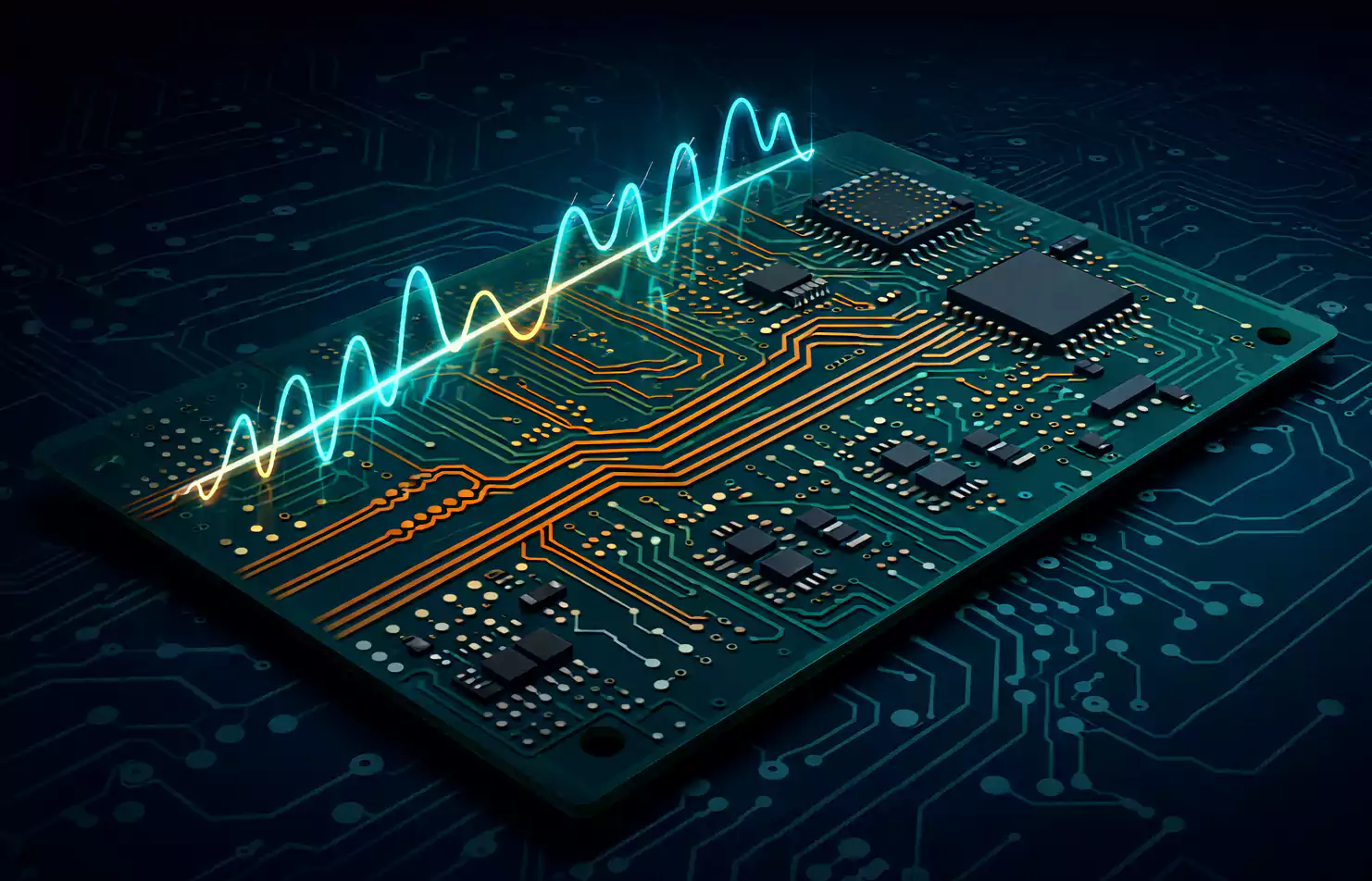
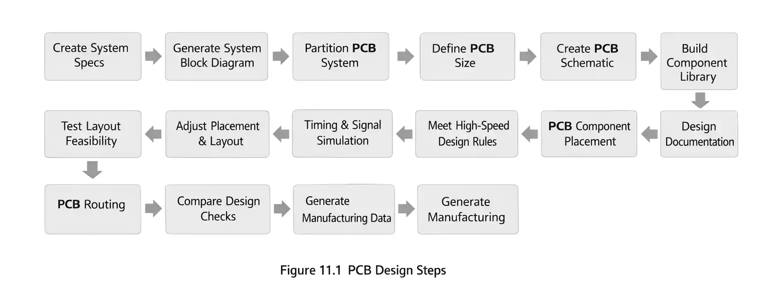
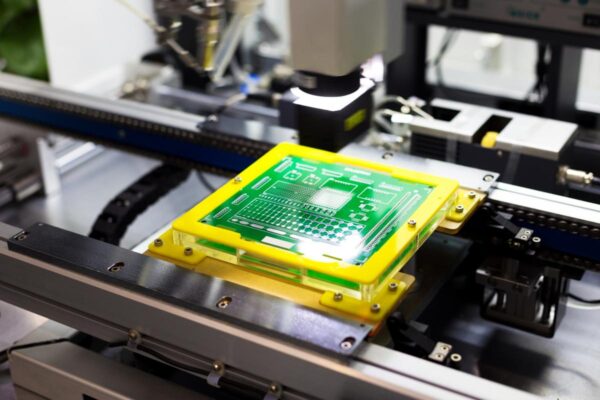
Many see PCB design as drafting—capture schematics, place components, route traces, send Gerbers—but that approach leads to costly redesigns and delays.
However, powering on is only the start. In commercial or industrial settings, a successful PCB must operate reliably despite component tolerances, material variations, temperature fluctuations, voltage swings, and manufacturing deviations. PCB Design Flow should also create full documentation for fabrication, assembly, testing, and maintenance.
As products shrink and integrate, PCB design evolves into a system-level discipline. This guide covers the start of the process: system definition, partitioning, library development, simulation, and layout.
The Real Objective of a PCB Design Flow
A disciplined PCB design flow ensures reliability and manufacturability.
1. Reliable Operation Under Real-World Conditions
A PCB must function not just under nominal conditions, but within realistic operating limits, including:
- Component value tolerances
- Device speed variations
- Material and laminate tolerances
- Operating and storage temperature ranges
- Power supply fluctuations
- Manufacturing dimensional tolerances
Ignoring these variables may result in lab-only functionality, leading to low yield, faults, thermal instability, or reliability issues during production or field operation.
Engineering for variation—rather than ideal conditions—is fundamental to a robust PCB design flow.
2. Complete Engineering Deliverables
A finished PCB design must produce more than layout files. It must generate a complete engineering package, including:
- Fabrication files
- Assembly data
- Test documentation
- Support data for troubleshooting and lifecycle management
In B2B settings, the deliverable is a manufacturing-ready data set that enables repeatable production and quality control, not just a design file.
PCB Design Has Become a System-Level Responsibility
Modern electronic products—especially in communications, industrial control, and computing—demand more from PCB designers than just circuit connectivity.
Today’s boards must address:
- Mechanical size and weight constraints
- High-speed signal interaction with advanced ICs
- PCB thermal management
- Electromagnetic interference (EMI)
- Integration with enclosures and structural materials
- Functional consolidation within a limited space
In telecom infrastructure, PCB layout affects cooling, EMI, and system reliability; here, the PCB serves both electrical and mechanical roles.
The evaluation criteria for PCB design have expanded accordingly. Electrical correctness is necessary, but no longer sufficient.
Start With a Clear System Specification
Every successful PCB project begins with a well-defined system specification.
Before schematic capture begins, the engineering team should define:
- Functional requirements
- Operating conditions
- Cost targets
- Development schedule
- Budget constraints
- Service and maintenance expectations
- Technology platform
- Mechanical size and weight limitations
- Regulatory or compliance requirements
For example, in a portable device, weight, battery life, reliability targets, storage, OS compatibility, and cost all shape material choice, power design, thermal strategy, and parts selection.
In multi-disciplinary teams—where hardware, firmware, mechanical, RF, and manufacturing engineers work in parallel—a unified system specification prevents misalignment and reduces integration risk.
Defined boundaries early on reduce costly corrections and make PCB design flow more predictable.
Develop a System Block Diagram Before Board Design
Once specifications are defined, the next step is to create a high-level system block diagram.
The purpose of this diagram is to clarify:
- Major functional modules
- Interconnections between subsystems
- Signal and power relationships
- Interface boundaries
This step forces the team to handle complexity early, before any physical design decisions are made.
Modularization is particularly important because different circuit domains require different design approaches:
- Analog and digital circuits behave differently.
- Low-frequency and high-frequency designs require different layout strategies.
- Power electronics impose different constraints than signal processing sections.
By defining modules early, engineering teams can assign domain experts to specific functional areas while preserving clear integration interfaces.
This approach improves efficiency and reduces the risk of cross-domain interference during layout.
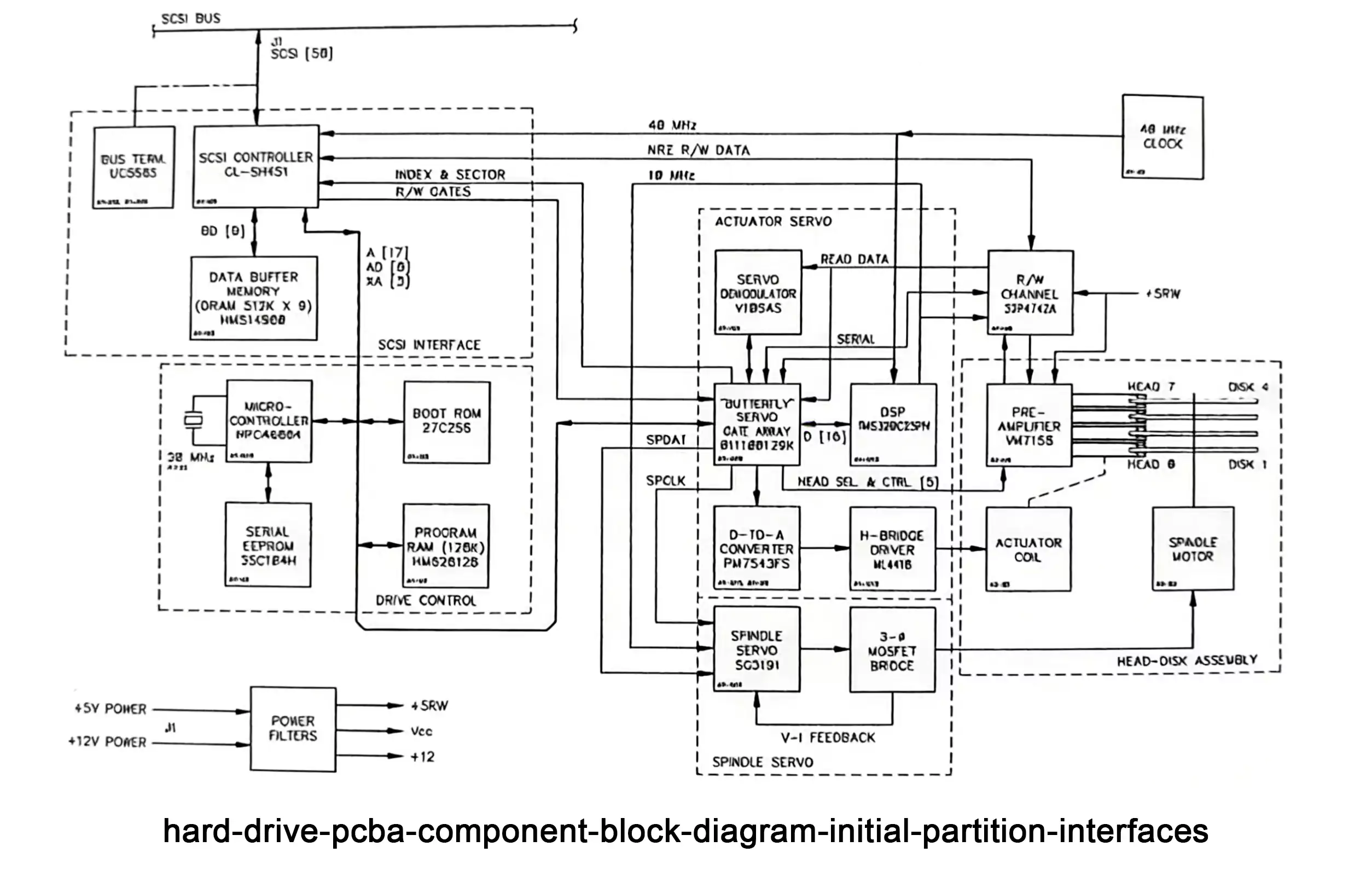
System Partitioning at the PCB Level
After functional decomposition, the next step is board-level partitioning.
Key decisions include:
- Which functions must reside on the same PCB?
- Which functions can be separated into daughter boards?
- How modules communicate (backplanes, buses, high-speed connectors)
In many systems, partitioning revolves around data buses and interface architecture. Some modules may be implemented as plug-in cards for serviceability or scalability. Others must remain tightly integrated for performance reasons.
Historically, analog and digital sections were often placed on separate boards. However, as miniaturization advances, many modern products integrate mixed-signal functions onto a single PCB. This trend requires careful control of thermal paths, grounding strategy, and PCB EMI design considerations.
Partitioning is no longer about isolation alone. It is about controlled integration.
Analog vs. Digital Design: Same Process, Different Priorities
Although analog and digital PCBs follow the same overall development process, their priorities differ.
In general:
- Analog circuits often operate at lower frequencies but with higher currents and power levels.
- Digital circuits increasingly involve high frequencies, fast edges, and tight timing margins.
These differences affect:
- Placement strategy
- Power distribution network design
- Grounding approach
- Thermal considerations
- EMI control methods
- Simulation focus
In mixed-signal systems, both design philosophies must coexist. Achieving stable performance requires balancing noise sensitivity, signal integrity, and power integrity within the same physical space.
This is also where practical PCB layout guidelines become essential, especially when analog and digital sections share one board.
Building a Robust Component Library
An organized component library is one of the most undervalued assets in PCB development.
Errors in footprints, pin mapping, or electrical attributes can lead to expensive assembly issues and redesigns. A properly structured component library should include:
- Package type (through-hole, QFP, BGA, CSP, etc.)
- Physical dimensions
- Pin pitch and pad geometry
- Pin numbering conventions
- Functional pin definitions (input, output, power, etc.)
- Relevant electrical characteristics
The benefits extend beyond convenience.
1. For Engineering Teams
- Reduced risk of footprint errors
- Consistent symbol and land pattern usage
- Improved collaboration across departments
- Faster design cycles
2. For Supply Chain
- Standardized part selection
- Reduced risk of sourcing bottlenecks
- Easier lifecycle management
3. For Product Evolution
- Simplified technology updates
- Controlled introduction of new packages and devices
In mature organizations, the component library is not just a design resource—it is a strategic engineering asset that supports a repeatable PCB design flow.
Simulate Before You Build
Physical prototypes are expensive. Simulation is not optional—it is a risk reduction tool.
Before committing to hardware, designs should be evaluated under realistic variations, including:
- Component tolerances
- Speed grade differences
- Operating temperature range
- Storage temperature limits
- Humidity exposure
- Voltage fluctuation
Traditional prototype-only validation often fails to cover edge cases, especially in complex systems. Design-stage simulation allows issues to be identified and corrected earlier, when changes are less disruptive.
Modern tools extend beyond functional circuit simulation. Many projects now incorporate:
- PCB thermal management analysis
- EMI evaluation
- Material thermal conductivity modeling
- Even enclosure-level interaction studies
Simulation shifts problem discovery forward in the development timeline—where it belongs.
Component Placement: Translating Logic Into Physical Reality
Once functional verification is complete, the design moves into physical layout.
Component placement bridges the gap between schematic intent and physical implementation.
Effective placement typically follows several principles and should be treated as part of broader PCB component placement guidelines:
- Group components by functional blocks
- Minimize critical signal path lengths.
- Keep interacting devices physically close.
- Position high-heat components for optimal thermal dissipation
- Place I/O circuitry near connectors.
This PCB Design Flow helps reduce routing complexity, improve signal behavior, and support downstream manufacturability.
Placement can be partially automated, but engineering judgment remains essential—particularly in high-density, high-power, or high-frequency designs.
Two Critical Placement Considerations: Thermal and EMI
Two issues often originate at the placement stage and are difficult to fix later: heat and electromagnetic interference.
1. Thermal Management
As IC power densities increase and board sizes shrink, PCB thermal management becomes a primary constraint.
Improper placement of high-power devices can lead to:
- Elevated junction temperatures
- Reduced reliability
- Performance degradation
- Field failure risk
Addressing thermal paths early—through placement, copper distribution, and airflow consideration—is often more effective than retrofitting heat sinks later.
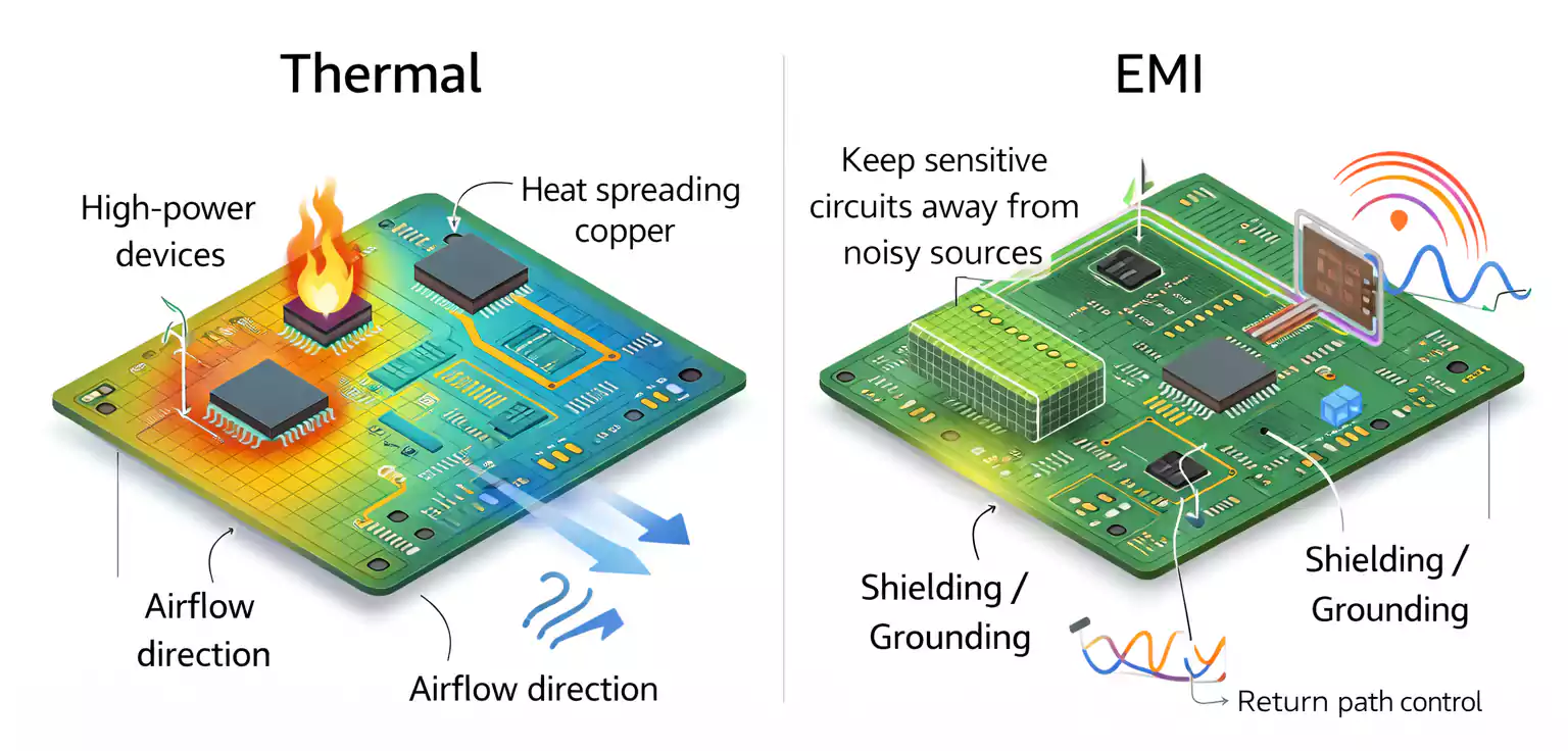
2. EMI Control
As operating frequencies increase, many components become increasingly sensitive to electromagnetic disturbances.
At the placement stage, engineers should consider these key PCB EMI design considerations:
- Separation between noisy and sensitive circuits
- Isolation of high-frequency modules
- Controlled return paths
- Shielding feasibility
In high-frequency systems, EMI stability often depends more on placement strategy than routing details. That is why both PCB EMI design considerations and PCB component placement guidelines should be addressed before detailed routing starts.
Closing Thoughts
The quality of the early PCB design flow largely sets the difficulty of everything that follows.
Clear specifications, sound partitioning, a clean library, meaningful simulation, and deliberate placement all reduce risk before copper is ever laid down. With that groundwork in place, high-speed constraints and routing become controlled engineering steps—not firefighting.
In the next part of this series, we focus on execution and walk through the high-speed PCB design flow from routing to manufacturing, including signal integrity, timing analysis, routability checks, and manufacturing files.