Introduction
What Is PCB Assembly (PCBA)?
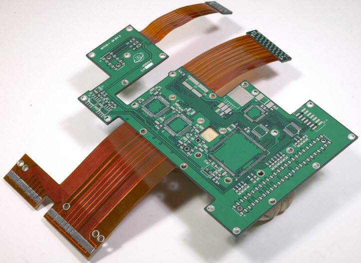
PCB Assembly, or PCBA, is the critical process that transforms a bare printed circuit board into a fully functional electronic module. By precisely soldering components—resistors, capacitors, ICs, connectors—onto copper-clad substrates, PCBA brings circuitry to life.
Unlike a fabricated PCB, which provides only the board’s physical structure and copper traces, a completed PCBA delivers reliable electrical performance ready for deployment in devices ranging from simple indicators to complex control systems.
PCB Fabrication vs. PCB Assembly
PCB fabrication and PCB assembly are two distinct but interdependent phases in turning a design into a working electronic device.
Fabrication creates the bare board—layering copper and dielectric materials, etching precise circuit patterns, drilling and plating holes, then applying solder mask and silkscreen. The result is a blank canvas defined by copper traces and vias, ready for components but not yet functional.
Assembly takes that fabricated board and brings it to life by soldering on resistors, capacitors, ICs, connectors, and more. Automated steps (solder-paste printing, pick-and-place, reflow) and manual techniques (through-hole insertion, wave or selective soldering) populate the board, while inspections (AOI, X-ray, ICT) and functional testing verify every joint.
When fabrication outputs (Gerber/ODB++ files, BOM, centroid data) seamlessly feed into assembly, you minimize errors, shorten lead times, and deliver reliable, high-performance PCBAs on schedule.
Why PCB Assembly Matters
High-quality PCB Assembly underpins product performance, longevity, and safety. In industries like medical devices, aerospace, and automotive electronics, even minor assembly defects can lead to costly failures or safety hazards.
Moreover, assembly often represents a significant portion of unit cost and production lead time—making process optimization and partner selection key drivers of project success.
What You’ll Learn in This Guide
In the sections that follow, you’ll gain:
- A thorough breakdown of SMT, through-hole, and mixed-technology workflows
- Best practices for pre-assembly preparation, quality assurance, and post-assembly finishing
- Insights into cost factors, component selection, and turnkey vs. consignment models
- Clear criteria for choosing the right assembly partner and answers to your most pressing FAQs
Whether you’re an engineer fine-tuning production or a decision-maker evaluating contract manufacturers, this guide delivers the actionable expertise you need to master PCB Assembly.
Terms & Types Overview
Quickly familiarize yourself with the six core PCB-assembly terms and four main assembly categories before diving into the full process.
Core Terms at a Glance
PCBA (Printed Circuit Board Assembly): The end product produced when electronic components are soldered onto a fabricated PCB, transforming it from a bare board into a functioning circuit.
SMT (Surface Mount Technology): Components (SMDs) are placed directly onto pads on the board surface without drilling holes. Enables higher component density, smaller footprints, and largely automated production.
THT (Through-Hole Technology): Components have leads inserted into pre-drilled holes and soldered on the opposite side, offering superior mechanical strength—ideal for connectors, large capacitors, and high-stress parts.
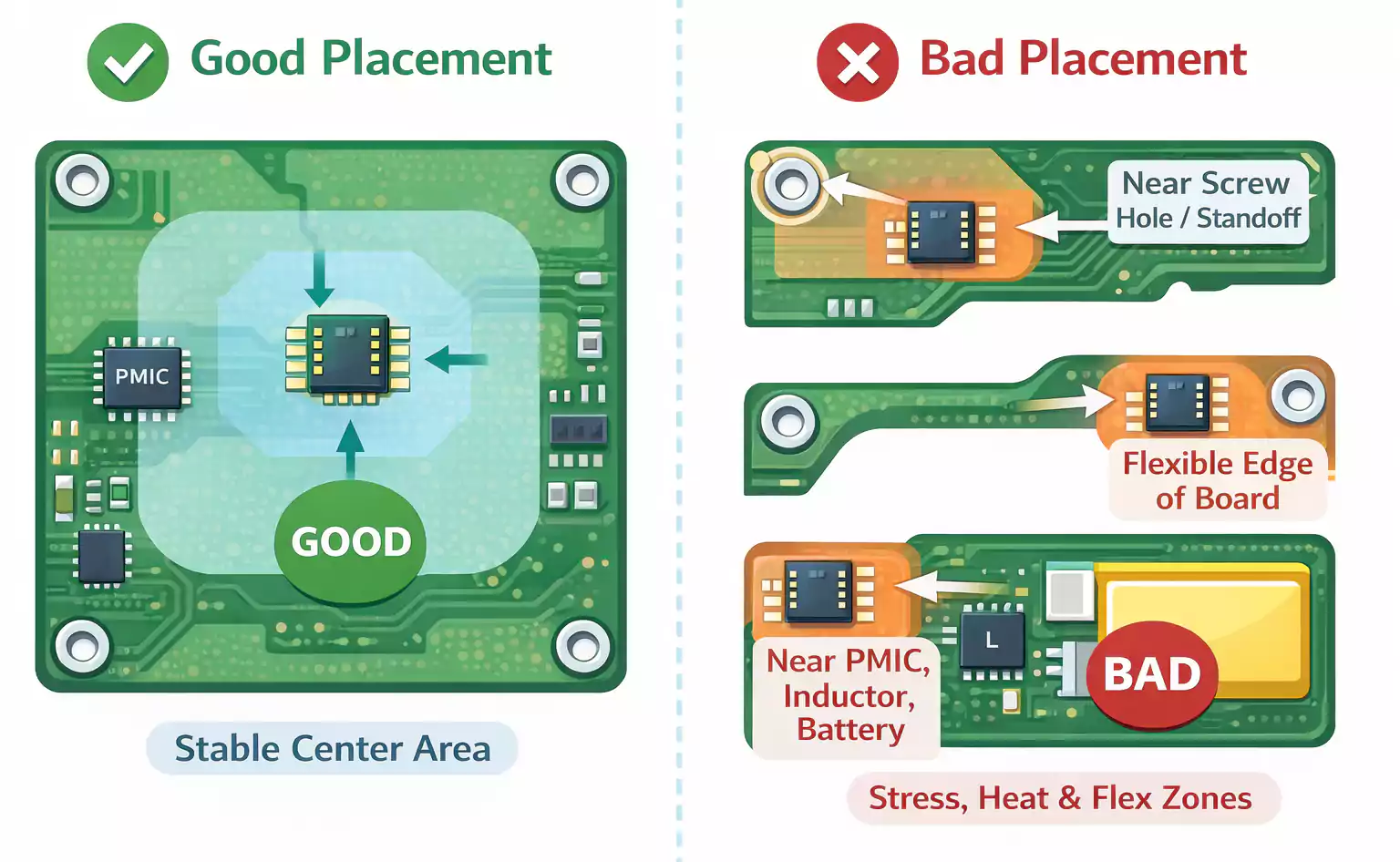
DFM (Design for Manufacturing): A set of guidelines and checks applied during PCB design to optimize dimensions, materials, and tolerances—minimizing production costs and avoiding manufacturability issues.
AOI (Automated Optical Inspection): High-speed camera systems scan assembled boards to detect solder-joint defects, missing or misaligned parts, and other surface anomalies—often used immediately after reflow.
ICT (In-Circuit Testing): Electrically probes individual nets and components on a PCB to verify correct soldering, continuity, impedance, and basic functionality before full functional testing.
Assembly Categories
| Category | Description | Typical Applications |
| SMT Only | Fully automated placement/reflow of surface-mount parts; no hole drilling required | High-volume consumer electronics, IoT devices |
| THT Only | Manual or wave soldering of through-hole components; provides robust mechanical support | Power supplies, industrial controls |
| Mixed (Hybrid) | Combines SMT and THT (and sometimes BGA) on one board; leverages both high density and strength | Complex PCBs in aerospace, medical equipment |
| Turnkey/Consignment | Turnkey: vendor sources all materials + completes assembly; Consignment: buyer provides some components | Rapid prototyping (consignment), full-service production (turnkey) |
With these terms and categories clear, you’re ready to explore each assembly workflow in depth—from stencil printing to final QA.
PCB Assembly End-to-End Process
Every successful PCB assembly begins long before any components touch copper. The development cycle starts with schematic capture and PCB layout, progresses through prototyping and design verification, and culminates in mass production preparation.
Early collaboration between design and manufacturing teams ensures that board stack-ups, material selections, and thermal profiles align with end-use requirements, minimizing costly design iterations downstream.
Pre-Assembly Preparation and Documentation
Before a single part is placed, three critical files must be validated:
- Gerber/ODB++ Files
These layer-by-layer artwork files dictate copper traces, solder mask openings, silkscreens, and drill locations. Automated checks confirm layer alignment, reveal missing data, and catch artwork errors.
- Bill of Materials (BOM)
A complete, accurate BOM lists part numbers, values, package types, approved vendors, and any alternates. Verifying each line item against component libraries prevents sourcing delays and mismatches.
- Centroid/Place Files
Pick-and-place machines rely on these X-Y coordinate files (with rotation and reference designator data) to mount surface-mount parts precisely. A quick test import into placement software flags coordinate or rotation inconsistencies.
A final DFM/DFA review cross-checks all files for manufacturability—ensuring trace clearances meet minimums, thermal reliefs are correctly applied, and component spacing allows for stencil apertures and pick-and-place access. By resolving these issues before fabrication, you drastically reduce the risk of board respins.
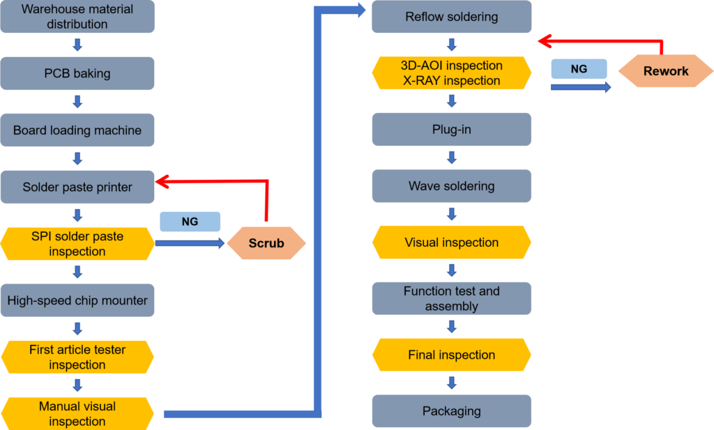
SMT Assembly Workflow
Surface-mount technology drives modern electronics manufacturing through a tightly sequenced chain of operations:
- Solder Paste Printing & SPI
A precision stencil deposits lead-free or leaded solder paste onto each pad. Immediately afterward, solder paste inspection (SPI) machines—using 2D height/area checks or full 3D volume scans—verify paste coverage and volume, catching misregistrations or bridges before they propagate errors downstream.
- Component Placement (Pick & Place)
High-speed pick-and-place machines retrieve reels of resistors, capacitors, BGAs, QFNs, and other SMD components, orient them correctly, and place them onto the pasted pads with sub-0.1 mm accuracy. Optimized feeder setups and pre-programmed nozzle change-overs ensure continuous throughput.
- Reflow Soldering
Boards advance through a multi-zone oven that gently ramps to soak, peaks above solder alloy melting point, and then cools under controlled conditions. Tightly profiled temperature curves prevent voiding, tombstoning, or thermal damage to sensitive parts.
- Automated Inspection & Electrical Testing
Post-reflow, automated optical inspection (AOI) systems scan for missing parts, tombstones, solder bridges, or misalignments. X-ray inspection validates hidden joints under BGAs and other concealed packages. Finally, flying-probe or in-circuit testing verifies net continuity, shorts, and opens—especially effective for prototypes and small batches where custom fixtures are impractical.
Through-Hole Assembly Workflow
Components requiring robust mechanical anchoring—such as connectors, inductors, and heavy capacitors—are handled in the through-hole stage:
- Component Insertion
Leads are either machine-inserted for high volumes or hand-inserted for small runs, ensuring proper seating depth and alignment.
- Wave and Selective Soldering
In wave soldering, boards pass over a turbulent S-shaped solder wave, soldering all through-hole joints in one rapid pass. For mixed-technology boards, selective soldering applies focused solder jets only to designated pins, protecting nearby SMT areas with custom masking or thermal profiling.
- Inspection and Rework
Technicians visually inspect solder fillets for proper meniscus and wetting. Any anomalies—cold joints, insufficient fillet height, or splashes—are manually reworked using temperature-controlled irons and fine-tip soldering tools.
Mixed-Technology Integration
Boards combining SMT and through-hole parts demand careful sequencing. The standard flow is SMT-first, completing paste printing, placement, reflow, and all SMT inspections before moving into THT insertion and soldering. This order prevents wave-solder heat from re-reflowing surface joints and introduces efficient production routing, with separate conveyor lanes for reflow ovens and wave-solder machines.
Post-Assembly Processing
Once all components are soldered:
- Cleaning & Non-Washable Component Soldering
Boards are cleaned—using aqueous or vapor-phase systems—to remove flux residues. Non-washable modules or connectors withheld earlier are now soldered with no-clean flux to avoid wet-process damage, followed by a secondary AOI and flying-probe test to confirm cleanliness and electrical integrity.
- Conformal Coating and Potting
For boards exposed to moisture, dust, or vibration, conformal coatings (acrylic, silicone, or polyurethane) or potting compounds are applied to protect solder joints and components, extending service life in harsh environments.
- Final Inspection (Visual, ICT, Functional Test)
A final visual inspection checks for cosmetic or mechanical defects. In-circuit testers (ICT) or flying-probe setups re-verify electrical nets under production-grade conditions. Finally, functional tests simulate real-world operation—powering the assembly, cycling inputs/outputs, and validating performance against design specifications.
By diligently following this end-to-end process—anchored in upfront data validation, rigorous SMT/THT execution, and multi-layered inspection—you ensure each PCBA meets stringent quality, reliability, and performance standards.
Quality Assurance & Inspection
Ensuring the integrity and reliability of every solder joint and component placement requires a tiered inspection strategy, blending human expertise with automated verification. Quality checks begin immediately after reflow soldering and continue through final functional testing, providing multiple “gates” that defects must pass before boards ship.
Visual Inspection
Highly trained operators perform the first review, examining solder fillets for proper wetting, fillet shape, and fillet height, as well as component orientation, polarity markings, and the absence of flux residues or contaminants. This manual check is critical for identifying gross defects—such as tombstoned parts, bridged leads, or lifted pads—that automated systems may miss.
Automated Optical Inspection (AOI)
Following visual confirmation, AOI systems use high-resolution cameras and pattern-matching algorithms to scan every board at line speed. AOI detects missing or misaligned components, solder bridges, insufficient solder, and lifted leads. By integrating AOI immediately after both solder-paste printing and reflow, you catch paste-related and joint-related defects before they propagate downstream.
X-Ray Inspection
For densely populated boards with BGAs, QFNs, and other hidden-joint packages, X-ray inspection provides non-destructive visibility into solder ball integrity, voiding, and head-in-pillow defects. Strategic X-ray sampling—whether full-board or key-device—ensures confidence in solder joints that cannot be observed optically.
Electrical Testing
- In-Circuit Testing (ICT): Using a “bed-of-nails” fixture, ICT applies controlled voltages and currents to confirm net continuity, component values, and the absence of shorts or opens. ICT is ideal for medium to high volume production runs.
- Flying-Probe Testing: For prototypes or low-volume batches, flying probes offer flexible, fixture-less testing. Programmable probes traverse the board to measure resistance, capacitance, and detect opens or shorts directly from the design netlist.
Functional Testing & Environmental Stress
After nets are verified, assemblies undergo functional test routines that mimic real-world operating conditions—power cycling, signal injection, and firmware validation. Boards destined for harsh or regulated applications receive additional environmental stress screening, such as thermal cycling and humidity testing, to expose early-life failures and verify long-term reliability.
By combining upfront data validation, layered optical and X-ray inspection, rigorous electrical testing, and environmental stress screening, you create a robust quality-assurance framework. This multi-gate approach not only minimizes rework and scrap but also delivers PCB assemblies with the performance and reliability demanded by today’s most exacting applications.
Value-Added Services
Firmware Programming & Burning
Our integrated firmware service ensures each board leaves the line fully loaded with your application code. Using JTAG, SPI, or UART interfaces, we batch-program custom bootloaders, encryption keys, and production firmware in a single pass. Engineers then run automated version-integrity checks so you receive assemblies that power up with the correct firmware every time, eliminating a separate post-assembly programming step and reducing your overall cycle time.
Product Certification & Reliability Testing
Navigating regulatory requirements can delay product launches. We manage the entire compliance journey—from UL and IEC safety assessments to IPC-A-610 workmanship audits—under one roof. In our environmental lab, boards undergo thermal cycling, salt spray, and vibration tests per ASTM and IPC standards. Upon completion, you receive a fully traceable test report, de-risking market entry and giving stakeholders confidence in your PCBA’s long-term performance.
Box Build & Electromechanical Assembly
Transform bare PCBAs into ready-to-deploy modules with our box-build service. We integrate chassis wiring, cable-harness assembly, and sub-system integration—outfitting enclosures, front panels, and connectors to your exact specifications. Each unit is then power-cycled and functionally tested as a complete system. By consolidating mechanical and electronic assembly under a single contract, you simplify logistics, cut lead times, and receive a turnkey solution tailored to your application.
Labeling & Laser Engraving
Permanent marking is essential for traceability and warranty management. We apply high-resolution laser engraving directly onto FR-4 boards or metal housings—embedding serial numbers, QR codes, and logos that resist abrasion, solvents, and extreme temperatures. Unlike adhesive labels, these laser-etched identifiers remain legible throughout your product’s lifecycle, streamlining asset tracking and compliance without risk of peeling or fading.
Cost Impact Factors
Managing costs in PCB assembly is critical—your choices around assembly methods, component technologies, and production volume will directly affect unit price and lead time. Below, we explore Manual vs. Automated Assembly, SMT vs. Through-Hole Components, and Production Scale, alongside a comparison table to help you quickly gauge trade offs.
Manual vs. Automated Assembly
For low-volume or irregular parts, manual assembly often incurs lower upfront expense since no specialized equipment is required. However, as volumes rise, labor costs escalate rapidly. Automated pick-and-place lines and wave-solder machines demand capital investment but, in medium to high volumes, dilute depreciation and labor costs—delivering lower per-unit prices and more consistent quality.
SMT vs. Through-Hole Components
SMT components are smaller, consume fewer raw materials, and benefit from bulk pricing, yet require investment in stencil printing and reflow ovens. Through-hole parts carry a slightly higher part cost and slower soldering rates (wave or hand), but provide superior mechanical strength for connectors and heavy components. Balancing part cost with assembly efficiency and mechanical requirements is key to optimizing overall cost.
Production Scale: Prototype → Small Batch → Mass Production
At the prototype stage, setup costs (programming, fixture creation, oven profiling) dominate, resulting in the highest per-board price. Small batches begin to spread these setup costs but still carry moderate labor rates. In mass production, setup costs are amortized across volumes, automation reigns, and per-unit cost reaches its lowest point—with the most predictable lead times. Always confirm minimum order quantities (MOQs) and typical cycle times with your assembler to align your budget and schedule.
| Production Scale | Setup Cost | Labor Cost per Board | Equipment Depreciation | Typical Lead Time |
| Prototype | High (fixtures & programming) | High (manual assembly) | Low | 1–2 weeks |
| Small Batch | Medium (partial amortization) | Medium | Medium | 2–4 weeks |
| Mass Production | Low (fully amortized) | Low (automation dominant) | High | 4–8 weeks |
Component Selection Recommendations
Selecting the right parts up front can significantly reduce procurement headaches, assembly costs, and quality risks. Below are three best practices—each with a brief explanation—followed by a concise summary table.
Reliable Vendor Sourcing
Always choose components from authorized distributors or directly from manufacturers with proven track records. This minimizes the risk of counterfeit or out-of-spec parts, ensuring consistent performance and avoiding production delays caused by quality rejections or backorders.
Standardize Package Families
Whenever possible, limit your design to a handful of common package types (e.g., 0603 resistors, 0805 capacitors, TQFP microcontrollers). Standardization streamlines your BOM, simplifies stencil and feeder setup, and reduces program-change time on pick-and-place machines—lowering both assembly complexity and costs.
Maximize SMT Usage
Favor surface-mount devices over through-hole wherever mechanical constraints allow. SMT parts are generally cheaper, smaller, and faster to place, enabling higher board densities and shorter cycle times. Reserve through-hole components only for connectors, high-power parts, or components with strict mechanical-strength requirements.
| Recommendation | Primary Benefit | Example Action |
| Reliable Vendor Sourcing | Ensures part authenticity and availability | Lock in suppliers with dual sourcing agreements |
| Standardize Package Families | Reduces setup time and BOM complexity | Use 0805 for all passive components where feasible |
| Maximize SMT Usage | Lowers part and assembly costs | Replace through-hole LEDs with SMD equivalents |
How to Choose an Assembly Partner
Selecting the right contract manufacturer (CM) is as critical as your design itself. The ideal partner not only executes your assembly flawlessly but also aligns with your production model, quality expectations, and budget. Below are four key considerations to guide your decision.
Turnkey vs. Consignment Model
In a turnkey arrangement, your CM sources all components, manages inventory, and handles procurement risks—ideal if you want a single point of accountability. Consignment, by contrast, lets you supply expensive or custom parts directly, reducing your upfront material spend but adding inventory-management overhead. Choose turnkey when you prioritize speed and simplicity; opt for consignment when you need tight control over high-value parts.
Production Volume & Flexibility
Different CMs specialize in different volumes. A partner geared for prototyping will excel at rapid turnarounds and low-volume runs but may charge premium rates for setup. Conversely, a high-volume manufacturer amortizes setup costs across thousands of boards, driving down per-unit cost but often requiring larger minimum orders. Match the CM’s typical batch sizes and minimum-order quantities with your forecasted volumes to avoid mismatches in cost or lead time.
Local vs. Overseas & Manufacturer vs. Electronics Distributor
Local CMs offer easier communication, faster shipping, and on-site visits—advantages when tight feedback loops and IP protection matter most. Overseas partners often provide lower labor rates and large-scale capacity but can introduce longer shipping times and language or cultural barriers. Similarly, selecting a dedicated manufacturer (with its own line equipment) versus an electronics distributor (who subcontracts assembly) determines your level of direct control over processes and quality. Prioritize local or direct-manufacturer CMs for complex, high-reliability projects; consider overseas hubs for mature designs with high volumes and longer lead-time tolerance.
Core Capabilities & Certifications
Assess each candidate’s equipment, certifications, and quality systems. Do they have advanced SMT lines, selective-solder machines, and in-house AOI, X-ray, and ICT? Are they ISO 9001 or IATF 16949 certified? Do they follow IPC-A-610 workmanship standards? A CM’s investment in modern equipment and rigorous quality management translates directly into fewer defects, higher yields, and more predictable deliveries.
By weighing these factors—business model, volume expertise, geographic and organizational structure, and technical credentials—you’ll be well-positioned to select an assembly partner that supports your product goals, protects your IP, and scales with your success.
FAQs
When should I choose a turnkey assembly model over consignment?
Turnkey is ideal if you prefer a single vendor to handle sourcing, inventory, and material risk. It streamlines logistics and places procurement responsibility on the assembler. Consignment makes sense when you need to supply specialized or high-value components yourself to control costs or guarantee authenticity.
What factors determine whether to use SMT or through-hole components?
Choose SMT for most parts when board density, size, and placement speed are priorities; it’s cost-effective in volume. Reserve through-hole for connectors, large capacitors, or components subject to mechanical stress, where lead strength outweighs the higher assembly time and part cost.
How can I verify a contract manufacturer’s quality capabilities without duplicating tests?
Request evidence of process control rather than repeating every inspection yourself. Review their calibration records, quality‐management certifications (e.g., ISO 9001, IATF 16949), and acceptance criteria for optical and X-ray inspections. A robust corrective-action process and historical yield data provide better insight than shadow-testing individual boards.
What typical minimum order quantities (MOQs) and lead times should I expect at different production stages?
Prototypes often carry MOQs as low as 1–5 boards with 7–14-day turnarounds. Small batches (10–100 boards) generally require MOQs around 10–50 boards and 2–4 weeks to ship. Mass production runs (hundreds to thousands) typically need MOQs in the hundreds and 4–8-week lead times, depending on material availability and assembly complexity.
How do I ensure firmware is correctly loaded before shipment?
Include programming instructions and firmware binaries in your assembly package. Confirm the assembler uses checksum or signature verification post-programming. A brief hardware-in-the-loop test—such as powering on and cycling critical functions—validates that the correct firmware version is present across the entire batch.
Accelerate Your Next PCB Project with Fast Turn
At Fast Turn, we deliver precision-driven, high-quality PCBA solutions with industry-leading turnaround times. Leverage our turnkey expertise—DFM review, prototype assembly, and end-to-end testing—to get your products to market faster and with complete confidence.
Appendix: Complete Glossary
Below is a comprehensive list of over 20 PCB-assembly terms and acronyms, presented alphabetically for quick reference.
| Term | Definition |
| AOI | Automated Optical Inspection: High-speed camera systems that scan assembled PCBs for surface defects such as missing or misaligned components. |
| BOM | Bill of Materials: A detailed list of every component, part number, value, package type, and approved vendor used in a PCB design. |
| CAM | Computer-Aided Manufacturing: Software tools that prepare PCB design data (Gerber/ODB++) for fabrication and assembly. |
| Conformal Coating | A protective polymer layer applied over assembled boards to guard against moisture, dust, chemicals, and vibration in harsh environments. |
| DFA | Design for Assembly: Guidelines and checks to ensure component placement, spacing, and orientation facilitate efficient, error-free assembly. |
| DFM | Design for Manufacturability: Reviews of PCB layouts to verify trace widths, clearances, and other parameters align with a manufacturer’s capabilities. |
| DRC | Design Rule Check: Automated verification of layout rules (clearances, hole sizes, layer counts) to catch violations before fabrication. |
| EDA | Electronic Design Automation: Suites of software used for schematic capture, PCB layout, simulation, and data export for fabrication. |
| FPT | Flying-Probe Test: Flexible, fixture-less electrical testing method that uses movable probes to verify continuity, shorts, and component values. |
| Gerber | Industry-standard file format that defines each PCB copper layer, solder mask, and silkscreen in vector graphics for fabrication. |
| ICT | In-Circuit Test: Bed-of-nails fixture testing that applies voltages/currents to individual nets and components to verify electrical integrity. |
| IPC A 610 | A global standard for PCB workmanship and acceptability criteria, covering solder joints, component placement, and board cleanliness. |
| JTAG | Joint Test Action Group: Interface standard used for boundary-scan testing and firmware programming via a serial test access port. |
| ODB++ | Enhanced data format combining Gerber, drill, net-list, and BOM information for seamless data transfer between PCB designers and manufacturers. |
| PCB | Printed Circuit Board: The bare board consisting of insulating substrate, copper traces, and drilled/plated holes—ready for component assembly. |
| PCBA | Printed Circuit Board Assembly: The completed board on which all components have been soldered, tested, and readied for deployment. |
| Pick and Place | Automated machines that retrieve components from reels or trays, orient them, and deposit them accurately onto solder-pasted PCB pads. |
| QFN | Quad-Flat No-Lead: A surface-mount IC package with leads arranged around the perimeter underside, requiring X-ray or cross-section inspection. |
| QFP | Quad-Flat Package: A surface-mount IC package with gull-wing leads on all four sides, commonly used for microcontrollers and logic ICs. |
| Reflow | The process in which solder paste melts under controlled thermal profiles to form reliable solder joints between components and PCB pads. |
| Silkscreen | The printed layer on a PCB that shows component reference designators, polarity markers, logos, and other assembly information. |
| SPI | Solder Paste Inspection: Equipment that measures solder-paste deposition (height, area, volume) after stencil printing to ensure correct paste application. |
| SMT | Surface Mount Technology: Assembly method where components are mounted directly onto the PCB surface without through-hole leads. |
| Stencil | A thin metal sheet with apertures matching pad layouts, used to deposit solder paste precisely during the SMT process. |
| THT | Through-Hole Technology: Assembly method where component leads are inserted into drilled holes and soldered on the opposite side for added strength. |