10L-HDI-PCB

Advanced 10-Layer HDI PCB with Selective Hard Gold & Blind/Buried Vias


Blind/Buried Hole (1-2,2-3,3-8,8-9,9-10)
Material FR4 Hi-Tg 170
Thicknes 1.6mm +/-10%
Panel size 86 x 43mm(1-up)
Width/space Partly 3/3mil line
Surface Treatment

Standard

Hole Wall Copper Thickness

Slective 30μ" Hard Gold + ENIG

IPC3

25 μm

This 10-layer HDI PCB, manufactured by Fastturn PCBs, showcases a high-performance multilayer design with precise microvia structures and premium surface treatments. Engineered for space-constrained and high-reliability applications, this board meets IPC Class 3 standards and offers excellent electrical performance.

Key Specifications:

  • Layers: 10

  • Blind/Buried Vias: (1-2, 2-3, 3-8, 8-9, 9-10)

  • Material: FR4, High-Tg 170

  • Board Thickness: 1.6 mm ±10%

  • Panel Size: 86 x 43 mm (1-up)

  • Line Width/Spacing: Partly 3/3 mil

  • Surface Finish: Selective 30 μ" Hard Gold + ENIG

  • Hole Wall Copper Thickness: 25 μm

  • Standard: IPC Class 3

The design leverages advanced via technology and high-density interconnects to ensure optimal signal integrity and performance for mission-critical systems.

To fabricate this board, the following data and design specifications are required:

  • Complete Gerber Files (RS-274X format preferred)

  • Drill Files with clearly marked blind/buried via layers

  • Stack-Up Details, especially for HDI via planning

  • Material Selection Confirmation (FR4 Tg170 or equivalent)

  • Surface Finish Specification (ENIG + Hard Gold)

  • Impedance Control Requirements (if applicable)

  • Assembly Constraints (if selective plating areas are tied to assembly needs)

  • Quantity and Delivery Timeline

Note: Due to the complexity of HDI structures, DFM (Design for Manufacturability) checks are highly recommended before production.

Q1: What is the purpose of using both ENIG and hard gold selectively?
A: Selective hard gold plating is used in high-wear contact areas like edge connectors, while ENIG is used elsewhere to ensure solderability and cost-efficiency.

Q2: What are blind and buried vias, and why are they used here?
A: Blind vias connect outer layers to inner layers, and buried vias connect only internal layers. They reduce layer-to-layer interconnection paths, enabling higher density without increasing board size.

Q3: Can you support impedance control for this PCB?
A: Yes. Impedance control can be implemented based on provided stack-up and trace width/spacing data. Please submit impedance requirements with your design.

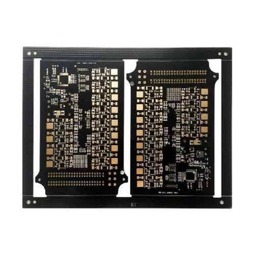
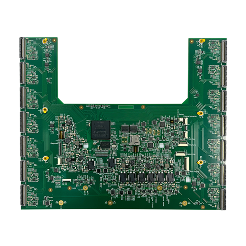
Q4: What applications is this HDI PCB best suited for?
A: This PCB is ideal for use in mobile devices, RF modules, high-speed computing, medical instruments, and aerospace-grade electronics where compact form factor and signal integrity are critical.

Q5: What is the minimum order quantity (MOQ)?
A: MOQ depends on specific production needs. We offer low-volume prototyping and high-volume production. Please contact us for a tailored quote.

Sharing is caring

Get in touch

Leave us a message

Please enable JavaScript in your browser to complete this form.