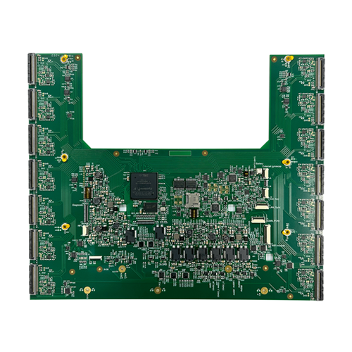
Q1: What is the main advantage of using a 32-layer PCB?
A: It allows for highly complex routing, better EMI performance, and separation of high-speed signals, power, and ground planes, essential in communication systems.
Q2: Why is impedance control critical in this board?
A: High-speed signals in communication devices require stable impedance to minimize signal distortion, crosstalk, and losses.
Q3: What challenges are associated with a 22:1 aspect ratio?
A: It demands precision in drilling and plating processes to maintain via reliability and overall board integrity.
Q4: Is back drilling essential?
A: Yes. Back drilling removes unused stubs from vias, which is crucial for signal integrity in high-speed designs.
Q5: Can this PCB be used in RF applications?
A: While it’s optimized for digital high-speed communication, with appropriate materials and layout, it can support certain RF applications as well.