Material | RO4350B (RO4450) |
Thicknes | 1.5-1.57mm |
Size | 214mm x 154mm |
Trace width min | 4.5mil |
Min Trace Distance
Min Drilling |
4.5mil
0.18mm |
Surface Treatment
Delivery time |
ENIG
8 Days |
Home - Case Studies - High-Frequency 10-Layer PCB with Rogers RO4350B
Material | RO4350B (RO4450) |
Thicknes | 1.5-1.57mm |
Size | 214mm x 154mm |
Trace width min | 4.5mil |
Min Trace Distance
Min Drilling |
4.5mil
0.18mm |
Surface Treatment
Delivery time |
ENIG
8 Days |
The 10-layer Rogers PCB is designed for high-frequency applications that demand exceptional signal integrity, low dielectric loss, and consistent performance across all layers. Utilizing RO4350B and RO4450 materials from Rogers Corporation, this PCB is ideal for RF, microwave, and high-speed digital circuits.
Key Specifications:
Material: Rogers RO4350B / RO4450
Layers: 10
Board Size: 214 mm × 154 mm
Board Thickness: 1.5–1.57 mm
Minimum Trace Width: 4.5 mil
Minimum Trace Spacing: 4.5 mil
Minimum Drill Size: 0.18 mm
Surface Finish: ENIG (Electroless Nickel Immersion Gold)
Standard Lead Time: 8 Days
Rogers materials are known for their high performance in demanding RF environments, offering superior thermal stability and low Dk/Df values compared to standard FR4.
To successfully fabricate this high-frequency multilayer Rogers PCB, the following design and production parameters were required:
Material Stack-up: Inclusion of RO4350B and RO4450 as per RF design specifications
Precise Trace/Spacing Control: Minimum 4.5 mil line width and spacing across high-frequency signal layers
Small Hole Drilling: 0.18 mm mechanical drilling capability to accommodate dense component layouts
Controlled Impedance Design: Critical for maintaining RF performance and signal quality
ENIG Finish: Selected for excellent surface flatness and solderability in RF assemblies
Consistent Thickness: Tolerance of 1.5–1.57 mm maintained throughout the board
Lead Time Requirement: Delivery completed within 8 working days
All boards comply with strict process control to ensure electrical and thermal consistency, especially vital in RF environments.
Q1: Why use Rogers RO4350B material instead of FR4?
A: RO4350B offers low dielectric loss and superior RF performance, making it ideal for high-frequency applications where FR4 cannot maintain signal integrity.
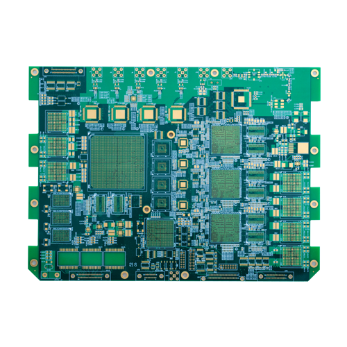
Q2: Can this board be used in both digital and RF hybrid applications?
A: Yes. The combination of RO4350B with RO4450 bonding layers allows for hybrid digital-RF circuits, making the board suitable for mixed-signal environments.
Q3: What’s the importance of tight trace width and spacing?
A: Minimum 4.5 mil trace/spacing ensures precise impedance control, essential for consistent signal transmission at high frequencies.
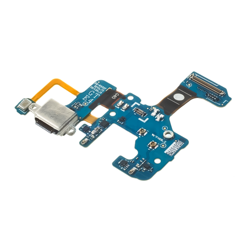
Q4: Is the ENIG surface finish suitable for RF boards?
A: Yes. ENIG provides a flat, reliable soldering surface and does not significantly impact signal loss at RF frequencies, making it a preferred choice for many designers.
Q5: Can Fastturn PCBs meet shorter lead times for Rogers boards?
A: Yes. While 8 days is the standard turnaround, expedited services may be available upon request depending on the design complexity.
Room 503, Building A03, Ping An Technology Silicon Valley, No. 76, Chuangyu Road, Ningxi Street, Zengcheng District, Guangzhou. 511358
1 Southwest Fifth Street, Dongguan City,China
Copyright 2025 © Fast Turn. All Rights Reserved.