Type | Communication Module Board |
Process | The strict stencil printing process |
Quality control |
Ensures the welding quality of the module |
Advantage |
The through rate reaches more than 99.5% |
Home - Case Studies - Communication Module Board
Type | Communication Module Board |
Process | The strict stencil printing process |
Quality control |
Ensures the welding quality of the module |
Advantage |
The through rate reaches more than 99.5% |
This Communication Module Board is designed for high-performance data transmission and signal processing in medical and industrial applications. Utilizing a precision stencil printing process, it ensures exceptional soldering quality and assembly consistency, delivering a remarkable production yield rate exceeding 99.5%.
Advanced stencil printing guarantees uniform solder paste deposition for fine-pitch and micro-scale components.
Optimized process control and inspection enable a >99.5% first-pass yield rate.
Suitable for use in medical communication interfaces, IoT modules, and embedded wireless systems.
Built to support high-frequency, low-noise performance with stable signal integrity.
Every board undergoes strict soldering quality checks, including AOI and functional tests.
To maintain performance and reliability in communication-critical systems, the following design and process standards are required:
Gerber files, BOM, stencil design (with aperture ratio data), Pick & Place files, and layout constraints.
Tight control of solder paste viscosity, stencil thickness, and printing alignment.
Automated Optical Inspection (AOI) and optional X-ray for modules with hidden solder joints.
Temperature- and humidity-controlled assembly environment for process consistency.
Use of RoHS-compliant materials and alignment with IPC-A-610 Class 2 or higher.
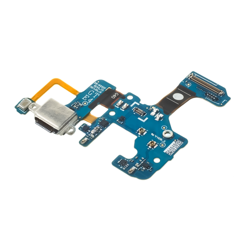
Q1: What is stencil printing and why is it critical for module boards?
A1: Stencil printing is the process of depositing solder paste on pads before component placement. For communication modules with fine-pitch pads, it ensures precise solder volume, critical for reliable connections.
Q2: What contributes to the >99.5% yield rate?
A2: The combination of controlled stencil printing, consistent solder paste quality, and real-time inspection systems ensures a high first-pass assembly yield.
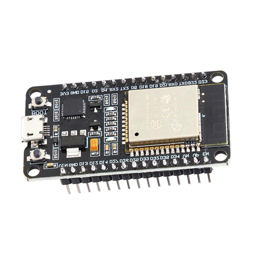
Q3: Can this board be used in wireless medical devices?
A3: Yes. It is ideal for wireless communication modules integrated into patient monitoring, wearable medical devices, and diagnostic tools.
Q4: How is soldering quality verified?
A4: Each unit undergoes AOI, and for complex packages, X-ray inspection is used to ensure complete and void-free solder joints.
Q5: What is the typical lead time for producing this module board?
A5: Lead times range from 2 to 4 weeks depending on complexity, customization, and component availability.
Room 503, Building A03, Ping An Technology Silicon Valley, No. 76, Chuangyu Road, Ningxi Street, Zengcheng District, Guangzhou. 511358
1 Southwest Fifth Street, Dongguan City,China
Copyright 2025 © Fast Turn. All Rights Reserved.