


Gold wire bonding is a mature, highly reliable interconnection method used in semiconductor packaging and PCB-based die assembly. But when bonding performance becomes inconsistent, the root cause is often not the bonding machine — it’s the PCB surface.
If your project involves Wire Bonding Gold Wire, two factors will directly impact your bonding yield and long-term reliability:
- Gold thickness on bond pads (minimum 2 µin / 2U)
- Surface finish structure (ENEPIG vs. ENIG)
This guide explains why 2U gold thickness is standard, how nickel exposure can lead to hidden failures, and why ENEPIG is a safer choice.
What Is Wire Bonding Gold Wire?
In PCB applications, gold wire bonding is commonly used for:
- COB (Chip-on-Board) assemblies
- Sensor modules
- LED modules
- RF and mixed-signal devices
- Custom hybrid circuits
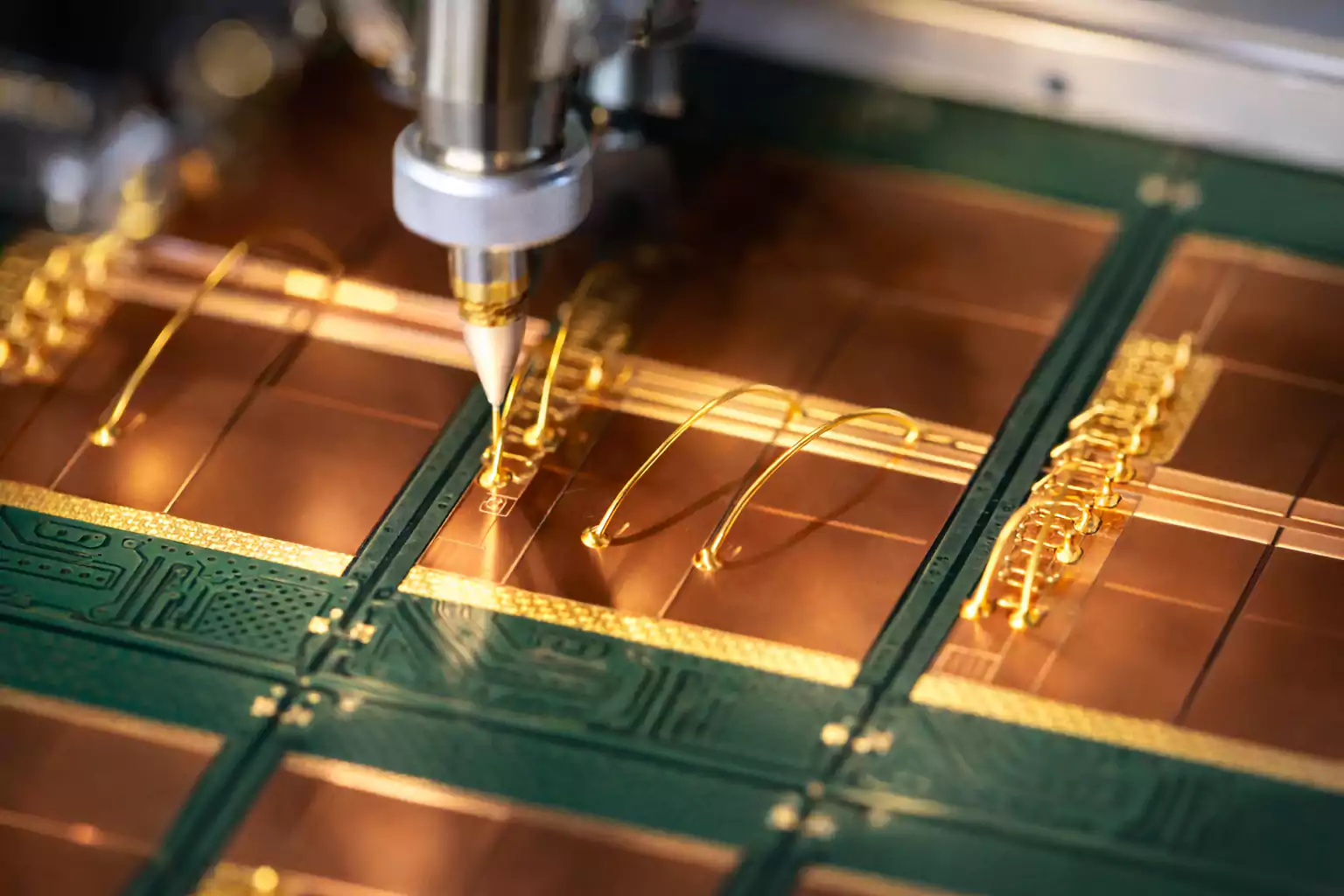
Unlike soldering, which uses molten metal, Wire Bonding Gold Wire is a solid-state process that uses controlled heat, pressure, and ultrasonic energy to form a metallurgical bond between a gold wire and a plated PCB pad.
Because the bond relies on metal-to-metal contact and atomic diffusion, surface condition and plating structure are more important than many engineers realize.
Ball Bonding vs. Wedge Bonding
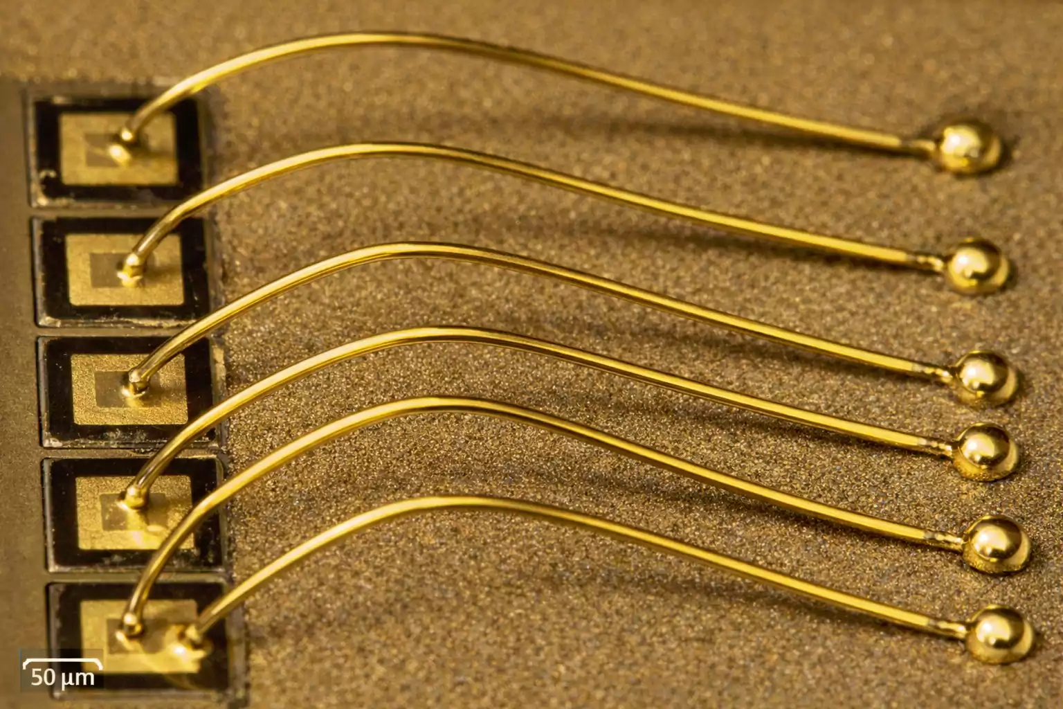
Most PCB gold wire applications use ball bonding (also called ball-stitch bonding):
- A small gold ball is formed at the tip of the wire.
- The ball is pressed onto a heated pad.
- Ultrasonic energy is applied.
- The first bond forms.
- The wire loops to the second pad.
- A stitch bond is created, and the wire is terminated.
This process involves localized deformation and microscopic scrubbing motion. That mechanical action is why gold thickness and surface integrity are critical.
Wedge bonding is used in certain applications, often with aluminum wire, but gold ball bonding dominates in most PCB-based die-attach environments.
Why 2U Gold Thickness Is the Practical Minimum
1. What Does “2U” Mean?
2U means 2 microinches (2 µin) of gold thickness.
That equals approximately 0.05 microns.
The thickness of gold plating in PCB fabrication is typically specified in microinches. When discussing 2U gold thickness for wire bonding, we’re referring to the immersion gold layer on ENIG or ENEPIG finishes.
2. Wire Bonding Is Not a Gentle Contact
During thermosonic bonding:
- The bonding head applies force.
- Ultrasonic energy introduces micro-scrubbing.
- Localized plastic deformation occurs.
This is intentional — the process breaks surface films and enables solid-state diffusion between metals.
However, if the gold layer is too thin, it can be disrupted or partially worn away during bonding.
When that happens, the underlying nickel layer becomes involved in the interface — and that’s where reliability issues begin.
3. Nickel Exposure: The Hidden Reliability Risk
Nickel exposure occurs when the gold layer is too thin or porous, allowing bonding energy to penetrate it.
When nickel becomes part of the bonding interface:
- Pull strength results become inconsistent.
- Shear values show wider variation.
- Bonding yield drops.
- Long-term reliability degrades under thermal cycling or humidity.
Nickel does not behave like gold at the bonding interface. It changes the process window and increases sensitivity to minor parameter shifts.
This is why a gold thickness of> 2 µm is considered a practical safety margin. It provides:
- Wear tolerance during ultrasonic bonding.
- A stable gold-to-gold interface
- Reduced risk of bonding variability
4. When You May Need More Than 2U
While 2U is often sufficient, some applications justify higher targets:
- Ultra-fine pitch bonding
- Higher ultrasonic energy settings
- Rework or rebond scenarios.
- Automotive or industrial high-reliability products
- Long-lifecycle devices exposed to thermal stress
In these cases, specifying both a minimum and a target gold thickness can further stabilize bonding yield.
Surface Finish for Wire Bonding: ENEPIG vs. ENIG
Gold thickness alone is not enough. The structure beneath the gold layer plays a major role in bonding performance.
The two most common finishes used for wire bond pads are:
- ENIG (Electroless Nickel Immersion Gold)
- ENEPIG (Electroless Nickel Electroless Palladium Immersion Gold)
1. ENIG and the Black Pad Risk
ENIG structure:
Copper → Electroless Nickel → Immersion Gold
In ENIG, immersion gold deposits directly onto nickel through a displacement reaction. Under certain chemical conditions, this process can attack nickel grain boundaries.
The result can be a brittle, phosphorus-rich layer — commonly referred to as a black pad.
In soldering applications, a black pad can cause brittle solder joints. In wire bonding, it can contribute to:
- Bond strength instability
- Interface inconsistency
- Increased variability in bonding yield
Modern ENIG processes are tightly controlled, but structurally, the gold is still deposited directly onto nickel.
2. Why ENEPIG Performs Better for Gold Wire Bonding
ENEPIG structure:
Copper → Electroless Nickel → Electroless Palladium → Immersion Gold
The key difference is the palladium layer.
Palladium acts as:
- A diffusion barrier
- A corrosion-resistant noble metal
- A protective layer over nickel
In ENEPIG, immersion gold deposits onto palladium, not directly onto nickel. This reduces the likelihood of nickel corrosion and significantly lowers the risk of black pad.
For high-reliability applications, ENEPIG offers a more stable interface and consistent bonding yield than ENIG.
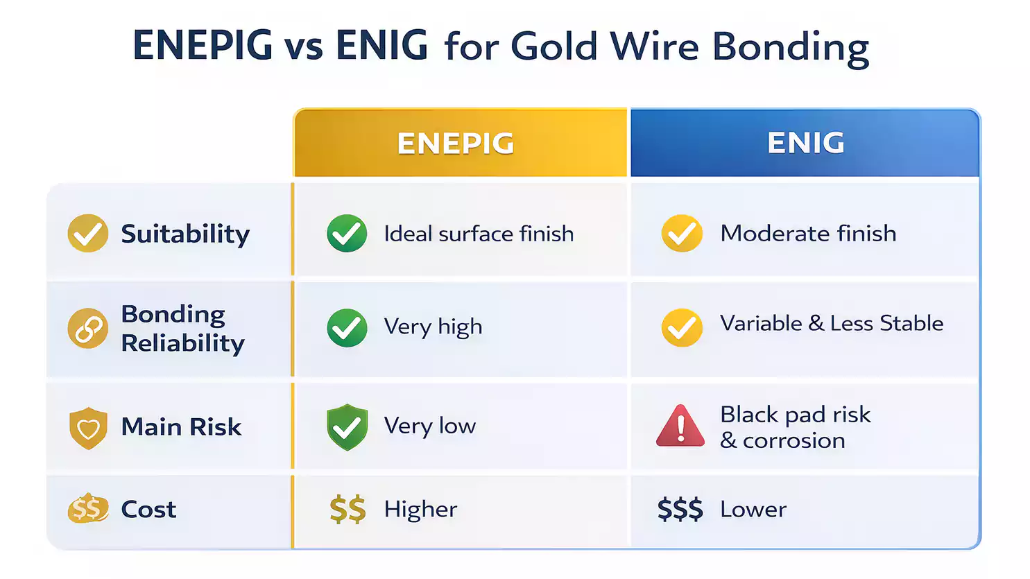
3. When Is ENIG Still Acceptable?
ENIG may be sufficient when:
- Reliability requirements are moderate.
- Bond pitch is not extremely fine.
- The fabricator maintains excellent process control.
- Cost constraints are significant.
However, when the priority is:
- Maximum bonding yield
- High wire bonding reliability
- Fine-pitch COB bonding
- Automotive or mission-critical electronics
ENEPIG is generally the safer and more conservative choice.
Other Factors That Affect Bonding Yield
Gold thickness and surface finish are foundational — but they are not the only variables.
1. Surface Cleanliness
Gold wire bonding is extremely sensitive to contamination:
- Organic residues
- Fingerprints
- Sulfur exposure
- Oxide formation
- Solder mask contamination
Even small amounts of surface contamination can narrow the bonding process window and lead to inconsistent yields.
Clean handling and proper packaging matter.
2. Pad Geometry and Mask Clearance
Poor pad definition can negatively affect bonding:
- Solder mask encroachment
- Uneven pad edges
- Insufficient clearance
- Surface irregularity
Fine-pitch bonding especially requires consistent pad flatness and geometry for uniform ultrasonic energy transfer.
3. Storage and Handling
Surface condition can degrade over time if not properly stored.
Best practices include:
- Controlled packaging
- Anti-sulfur storage environments
- Minimizing air exposure before bonding
- Avoiding unnecessary contact with bond pads
Surface stability directly impacts bonding reliability.
FAQ: Wire Bonding Gold Wire
What is the 2U gold thickness?
2U equals 2 microinches (2 µin), or approximately 0.05 microns. It represents a practical minimum thickness for stable gold wire bonding.
Why is ENEPIG preferred for gold wire bonding?
ENEPIG includes a palladium layer that protects nickel and reduces the risk of black pad. This leads to more stable bonding interfaces and higher yield consistency.
What is a black pad in ENIG?
A black pad is a corrosion-related defect in the electroless nickel layer that can weaken the bonding interface and cause variability in mechanical performance.
How do you prevent nickel exposure during bonding?
Specify adequate gold thickness (≥ 2U minimum).
Use ENEPIG for high-reliability applications.
Ensure proper PCB fabrication process control.
Avoid excessive ultrasonic energy outside the process window.
Final Thoughts
Wire Bonding Gold Wire is reliable but sensitive to variations in gold thickness and surface finish, which affect yield and long-term reliability.
For most PCB wire bonding applications:
- Gold thickness ≥ 2U should be considered a baseline requirement.
- ENEPIG is the safer choice over ENIG for reliability-critical applications.
- Preventing nickel exposure and minimizing black pad risk are critical to stable performance.
At FastTurnPCB, we work with customers to develop COB assemblies, fine-pitch modules, and high-reliability electronics, ensuring surface finish and gold thickness are specified correctly from the beginning. Getting these details right early can prevent costly yield losses later in production.
