

When designing or manufacturing a printed circuit board (PCB), one of the most essential yet often overlooked layers is the solder resist, also known as the solder mask. This thin polymer coating determines whether your PCB assembly process runs smoothly or ends in a mess of solder bridges and oxidation.
This comprehensive guide explains what solder resist is, why it matters, the types of solder resist materials, typical thicknesses, color options, and key design guidelines to avoid costly PCB defects.
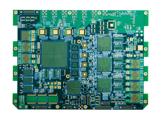
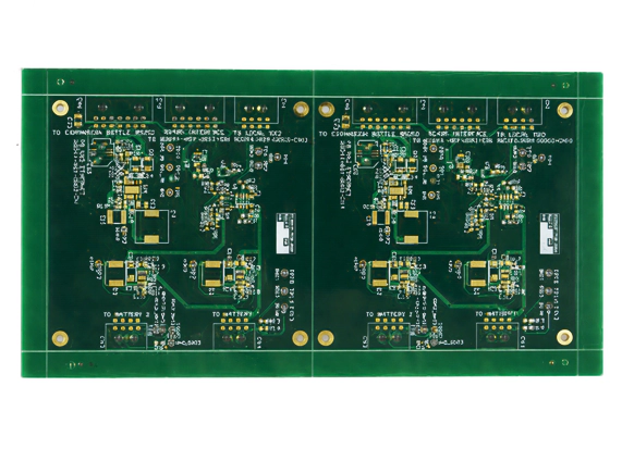
What Is Solder Resist?
In simple terms, solder resist is a protective polymer layer applied to the copper surfaces of a PCB, covering all areas except those intended for soldering, such as component pads or test points.
In your PCB design software (such as Altium, KiCad, or Eagle), this appears as a solder mask layer, typically with openings around pads and vias. In the manufacturing process, the solder resist prevents solder from flowing where it shouldn’t—especially between tightly spaced pads during wave or reflow soldering.
You’ll find it on both sides of the board:
- Top solder mask (the component side)
- Bottom solder mask (the opposite side)
In short, solder resist defines the “no-solder zone” on your PCB.
Why Use Solder Resist?
Without solder resist, molten solder would easily bridge across fine-pitch pads or vias, causing shorts and rework nightmares. Its main functions include:
- Prevent solder bridging: Maintains electrical isolation between adjacent pads during reflow or wave soldering.
- Protect copper: Shields copper traces from oxidation, corrosion, and environmental contamination.
- Improve durability: Adds a layer of mechanical and chemical protection against handling, cleaning, and moisture.
- Enhance manufacturability: Makes automated assembly and inspection more reliable by clearly defining where solder should go.
- Improve insulation: Adds an extra dielectric barrier, reducing the risk of leakage or electrochemical migration.
In short, solder resist isn’t just aesthetic—it’s a crucial reliability layer.
Types of Solder Resist
Solder resist can be categorized by application process and intended purpose.
1. Permanent Solder Resists (Used in PCB Fabrication)
• Liquid Photo-Imageable (LPI)
- Most common in modern PCB manufacturing.
- Applied by screen coating, curtain coating, or spraying.
- Photosensitive: exposed to UV light through a phototool and developed to form precise openings.
- Excellent for fine-pitch components and HDI boards.
• Liquid Epoxy (Screen Printed)
- Older, low-cost process using thermally cured epoxy ink.
- Thicker and less precise, but durable for simple, low-density boards.
• Dry Film Solder Mask
- Applied as a laminated sheet and photolithographically patterned.
- Delivers very uniform thickness and sharp edges, ideal for high-precision or military PCBs.
- More expensive and less flexible for uneven topography.
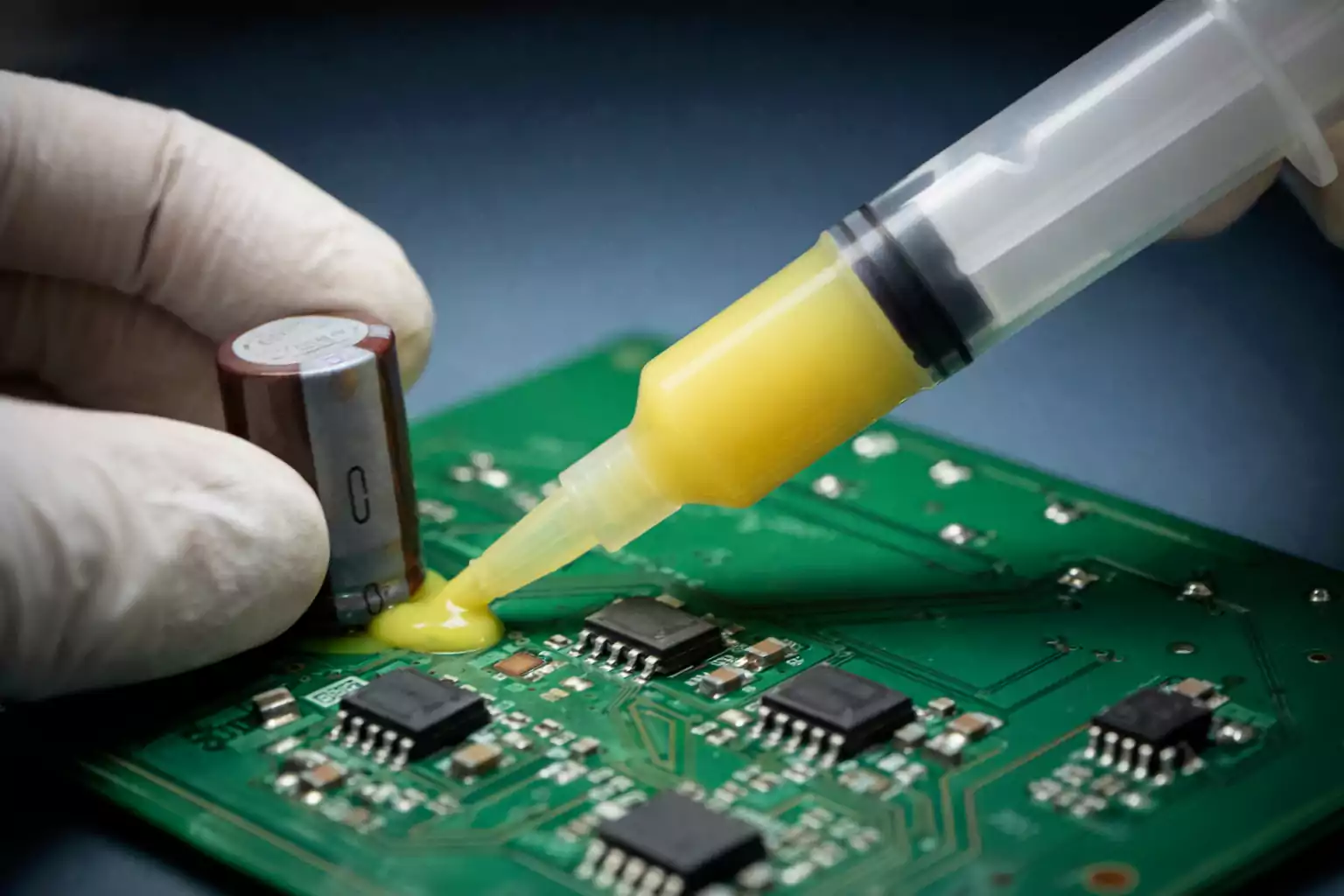
2. Temporary (Peelable) Solder Mask
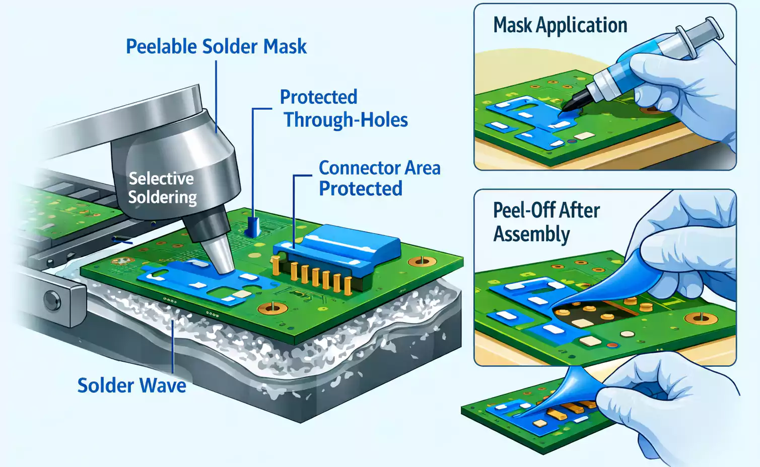
Used during assembly, repair, or selective soldering, the temporary solder mask is applied manually or by stencil and later peeled or washed off.
It protects areas you don’t want soldered or coated—for example, through-holes during wave soldering, or connector areas during conformal coating.
Temporary masks are typically latex- or acrylic-based and not part of the final PCB.
Solder Resist Materials and Key Properties
A solder resist material typically contains:
- Base resin: Epoxy or polyimide providing adhesion and dielectric strength
- Hardener/curing agent: Ensures mechanical durability and chemical resistance
- Photo-initiators: For UV exposure in LPI or dry-film systems
- Pigments and fillers: Control color, viscosity, and opacity
Important performance characteristics:
| Adhesion | Prevents delamination during reflow or cleaning |
| Heat resistance | Must withstand >250 °C during reflow |
| Chemical resistance | Must survive flux, solvent, and conformal coating exposure |
| Electrical insulation | High dielectric strength (>500 V/mil typical) |
| Moisture resistance | Limits ionic contamination and leakage |
Material selection tips:
- For fine-pitch HDI boards: use LPI with laser-direct imaging (LDI) capability.
- For automotive or power-electronics applications, choose high-temperature or chemically resistant epoxy systems.
- For flex or rigid-flex PCBs: use flexible coverlay films instead of rigid solder mask.
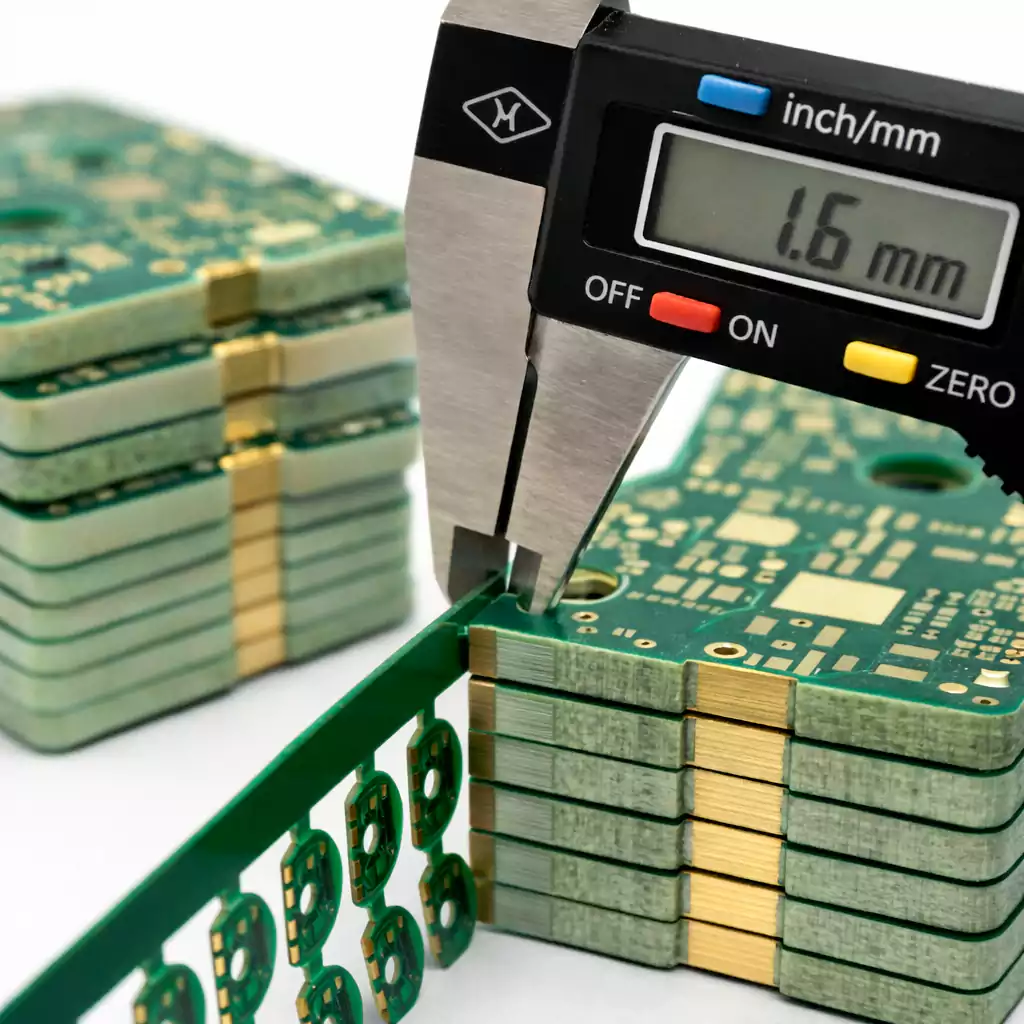
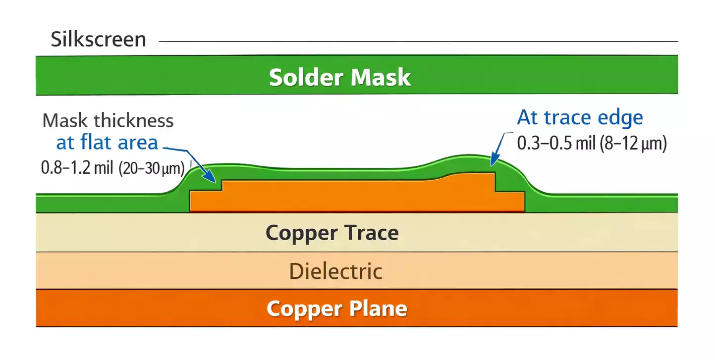
Typical Solder Resist Thickness
The thickness of solder resist varies depending on application method, board layout, and surface features.
| Flat copper areas | 0.8 – 1.2 mil (20–30 µm) |
| Trace edges and corners | 0.3 – 0.5 mil (8–12 µm) |
| Solder mask dam between pads | ≥ 4 mil (100 µm) width recommended |
Too thin? You risk exposing copper, oxidation, or electrical leakage.
Too thick? The mask can cause poor solder wetting or interfere with component seating.
Uniformity is key. Manufacturers often measure thickness at multiple cross-sections to ensure compliance with IPC-SM-840.
Solder Resist vs. Solder Mask: Are They the Same?
Yes. In modern PCB terminology, “solder resist” and “solder mask” are interchangeable.
The term resist emphasizes the coating’s role in resisting molten solder, while mask reflects its photolithographic patterning nature.
In design files (Gerber format), this appears as:
- Top solder mask layer (.GTS)
- Bottom solder mask layer (.GBS)
Both define where solder resist is absent, not where it exists.
Permanent vs. Temporary Solder Resist
| Purpose | Long-term protection on finished PCB | Temporary protection during assembly |
| Applied by | Fabricator | Assembler or technician |
| Curing | UV + thermal | Room temp or mild heat |
| Removal | Permanent | Peeled or washed away |
| Examples | Green mask on PCB | Blue latex mask for selective soldering |
Permanent masks define the circuit’s solderable pattern; temporary masks protect specific zones during processing.
Solder Mask Color: Why Is It Green?
Ever wondered why almost every PCB you see is green? There are both technical and practical reasons.
Why green dominates
- Best process visibility: Green offers excellent contrast against copper and silkscreen, making inspection and AOI (automated optical inspection) easier.
- Mature process control: Manufacturers have optimized curing and imaging for green resins, ensuring consistent quality and low defect rates.
- Thermal and chemical stability: Green pigments typically withstand reflow and cleaning chemicals better than other colors.
Other colors and trade-offs
| Black | Sleek look, hides traces | Poor contrast, traps heat |
| White | Used in LEDs & lighting | Reflects light, but yellows easily |
| Red / Blue | Good for prototypes or branding | Slightly wider tolerances |
| Transparent | For high-frequency RF boards | Exposes copper appearance |
Color choice doesn’t significantly affect electrical performance—but it can impact inspection accuracy and yield.
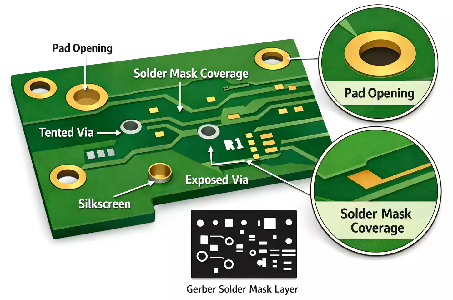
Visual Guide: Solder Resist and Common Defects
Understanding what “good” and “bad” solder resist looks like helps catch problems early.
Typical patterns:
- Pad openings: Circular or rectangular exposed copper zones for soldering.
- Tented vias: Covered vias to prevent solder wicking.
- Solder dams: Narrow strips between pads, preventing bridging.
Common defects to watch for:
| Misregistration | Mask offset covering pad edges | Alignment error or improper expansion |
| Slivers / broken dams | Narrow mask strips detached | Too small mask web (< 4 mil) |
| Bubbles or pinholes | Air or contamination during coating | Inadequate cleaning or degassing |
| Peeling or delamination | Mask lifts after reflow | Poor adhesion or improper cure |
| Uneven color or gloss | Non-uniform thickness | Coating or curing variation |
Design Guidelines (DFM Rules)
1. Solder Mask Expansion
In CAD tools, solder mask openings are typically expanded by 2–4 mil around each pad to account for alignment tolerance.
Too little expansion → risk of mask covering pad edges.
Too much → solder bridging between pads.
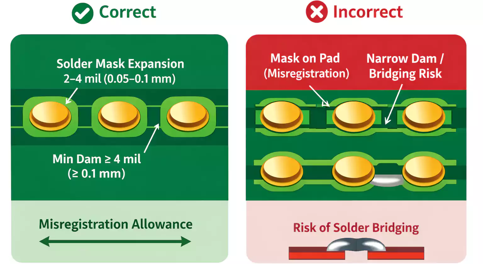
2. Minimum Solder Mask Dam (Web)
Keep at least 4 mil between adjacent pads after mask expansion.
For darker colors (like black), increase to 5 mil to account for lower imaging tolerance.
3. Via Treatment
- Tented vias: cover via holes completely to prevent solder wicking.
- Plugged vias: filled with resin, used under BGAs.
- Open vias: left exposed for testing or thermal reasons.
4. Communication with Your Fabricator
Include solder mask notes in your fabrication drawing:
- Mask type (LPI, color, gloss)
- Expansion rules
- Via the tenting/plugging requirements
- IPC class (usually IPC-SM-840 Type T, Class 2/3)
Troubleshooting and Repair
Even well-controlled processes can show defects.
Here’s how to interpret and fix them:
| Mask peeling or blistering | Contaminated copper, poor adhesion | Improve cleaning or pre-bake |
| Mask misalignment | Artwork or exposure offset | Adjust registration settings |
| Slivers or missing mask | Mask dam too narrow | Increase web width in layout |
| Oxidized copper under mask | Incomplete cure or voids | Review UV/thermal profile |
| Need to access copper (rework) | Design change or test pad | Use controlled mask removal (see below) |
How to Remove Solder Resist (for Rework)
In rework or circuit modification, removing solder resist may be necessary.
Common methods include:
- Mechanical scraping: For small local areas—use a precision fiberglass pen or scalpel.
- Micro-abrasion (microblasting): Uses a fine powder to erode the coating gently.
- Chemical stripping: Specialized solvents remove the cured resin (best left to professionals).
- Laser ablation: Precise but expensive; used for HDI rework.
Always avoid damaging the underlying copper. Removing solder mask changes surface roughness, solderability, and potentially impedance on high-speed traces.
FAQ
Is solder resist the same as solder mask?
Yes, the two terms are interchangeable; “resist” highlights its anti-solder property, “mask” its photolithographic role.
What is solder resist made of?
A mix of epoxy or polyimide resin, hardener, photo-initiator, and pigment for color and durability.
What is the standard thickness of solder mask?
Typically 0.8–1.2 mil (20–30 µm) in flat areas, thinner at edges.
Why is the solder mask green?
Green provides the best optical contrast and process control, giving higher inspection accuracy and yield.
What is the minimum solder mask dam width?
Usually 4 mil (100 µm) minimum; increase to 5 mil for black or white masks.
When should I tent or plug vias?
Tent small vias to prevent solder wicking; plug only when vias sit under BGA pads or in critical thermal zones.
Can I remove solder resist?
Yes, for rework or testing—but only with controlled mechanical or chemical methods to avoid damaging copper.
Does solder mask color affect performance?
Not electrically, but it affects optical inspection and heat absorption. Green generally yields the best results.
Conclusion
Solder resist may look like a simple colored coating, but it’s a critical layer that defines your PCB’s manufacturability, reliability, and longevity.
Understanding its materials, thickness, design rules, and color implications helps you communicate better with your PCB fabricator and design boards that are both robust and production-ready.
In short, a well-designed solder resist layer is not decoration—it’s engineering precision you can see.
