


Introduction
When designing or manufacturing a printed circuit board (PCB), one critical but often overlooked element is the solder mask. Also known as solder resist, this thin protective layer plays a vital role in both the functionality and durability of a PCB. Whether you're a design engineer, PCB fabricator, or electronics hobbyist, understanding what a solder mask is—and how it affects performance, reliability, and manufacturability—is essential.
At its core, the solder mask is a polymer-based coating that is applied over the copper traces on a circuit board to prevent solder bridges, protect against oxidation, and improve electrical insulation. You’ve likely seen it as the green coating on most PCBs, although it comes in many colors and types depending on the application.
In this guide, we’ll go far beyond a basic definition. You’ll learn about the different solder mask materials, their manufacturing processes, key design rules, signal integrity considerations, and common failure modes.
What is Solder Mask?
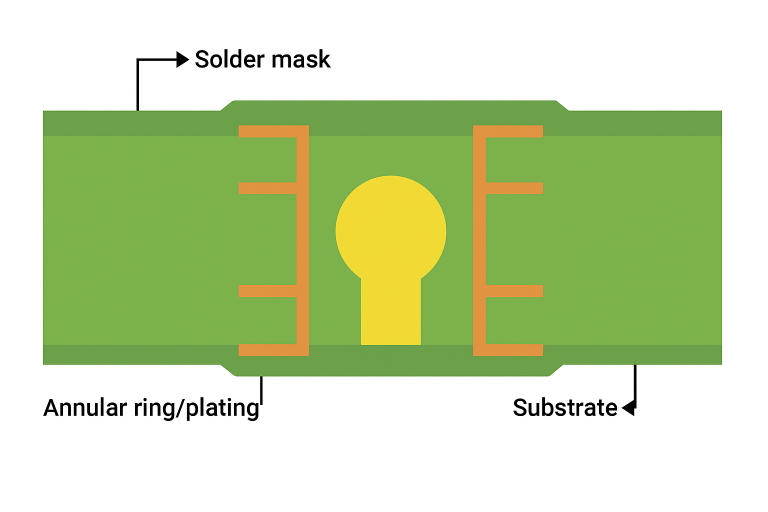
A solder mask, also known as solder resist or solder stop, is a thin protective polymer layer that covers the copper traces of a printed circuit board (PCB). Its primary purpose is to prevent solder bridging during assembly and to protect exposed copper from oxidation, moisture, and contamination. Without a solder mask, molten solder could flow uncontrollably across the board, causing short circuits and reliability issues.
In PCB manufacturing, the solder mask is typically applied to both the top and bottom layers of the board, leaving only the necessary pads, vias, or component connection points exposed. This selective coverage ensures precise soldering while keeping the rest of the copper circuitry insulated and safe.
Key Functions of Solder Mask
- Prevents solder bridges by insulating fine copper traces during reflow soldering.
- Protects copper from corrosion and environmental exposure.
- Improves insulation and reduces the risk of electrical leakage between conductors.
- Enhances mechanical strength, helping prevent copper trace lifting or peeling.
- Improves aesthetics, giving PCBs their characteristic green or other color finish.
Solder Mask vs. Paste Mask
One common source of confusion is the difference between solder mask and paste mask.
- Solder mask: A permanent protective coating that insulates most of the PCB surface.
- Paste mask (stencil layer): A temporary opening layer used during assembly to define where solder paste is applied for component placement.
In short, the solder mask is for long-term PCB protection, while the paste mask is for accurate solder paste deposition during assembly.
Common Colors and Their Role
Although green solder mask is the industry standard due to its cost-effectiveness and ease of inspection, PCB manufacturers also offer red, blue, black, white, and even transparent solder masks. Color does not significantly affect electrical performance, but it may impact inspection visibility, aesthetics, and light reflection—which can be important for certain applications such as consumer electronics or LED boards
Solder Mask Materials
When it comes to printed circuit boards (PCBs), the choice of solder mask material directly impacts manufacturability, reliability, and even electrical performance. Understanding the different types of solder mask materials helps designers and engineers make informed decisions based on cost, functionality, and end-use requirements.
1. Common Types of Solder Mask Materials
1.1 Liquid Photo-Imageable (LPI) Solder Mask
- Most widely used in modern PCB manufacturing.
- Applied as a liquid coating through screen printing, spraying, or curtain coating.
- Exposed to UV light with a phototool, which defines the solder mask openings.
- Offers high resolution, fine pitch capability, and good adhesion.
- Well-suited for HDI boards, BGA designs, and other high-density layouts.
1.2 Dry Film Solder Mask
- A laminated film applied to the PCB surface and then photo-imaged.
- Provides excellent thickness control and mechanical strength.
- Less common today due to higher cost and limited adaptability for very fine pitches.
- Still useful in specialized applications where uniform thickness and rigidity are critical.
1.3 Epoxy-Based Screen-Printable Ink
- Traditional solder mask type, often applied with silk-screen printing.
- Lower cost and simple processing make it attractive for low-volume or prototype boards.
- However, resolution is lower compared to LPI, and it is not ideal for high-density interconnects.
1.4 Specialized Low-Loss and High-Frequency Materials
- Designed for RF and microwave PCBs, where dielectric constant (Dk) and dissipation factor (Df) play critical roles.
- These solder masks minimize signal loss and are compatible with high-frequency substrates such as Rogers or PTFE laminates.
- More expensive, but essential for 5G, automotive radar, and aerospace communication boards.
2. Key Performance Properties to Consider
When evaluating solder mask materials, designers should look at:
- Adhesion strength: Ability to bond to copper and laminate.
- Thermal resistance: Withstand solder reflow and operating temperatures.
- Dielectric properties: Low Dk and Df are crucial for high-speed PCBs.
- Chemical resistance: Protect against flux, cleaning agents, and environmental factors.
- Thickness and uniformity: Prevent defects like bridging or insufficient coverage.
- Cost vs. performance balance: Choosing materials that fit the project budget without sacrificing quality.
3. Solder Mask Material Comparison Table
| Material Type | Advantages | Limitations | Best Use Cases |
|---|---|---|---|
| LPI | High resolution, cost-effective, flexible application | Requires precise process control | HDI boards, consumer electronics |
| Dry Film | Uniform thickness, strong mechanical properties | Higher cost, less adaptable to fine pitch | Specialty boards, military/industrial |
| Epoxy Ink | Low cost, simple processing | Low resolution, poor for fine pitch | Prototypes, low-volume boards |
| Low-Loss HF Materials | Excellent electrical properties, low signal loss | Expensive, specialized | RF, microwave, aerospace, 5G |
4. Material Selection Tips
- For standard consumer electronics, LPI is the best balance of cost and performance.
- For high-density or fine-pitch designs, LPI outperforms older epoxy inks.
- For military or industrial applications requiring robust coatings, dry film may be preferred.
- For high-frequency circuits, invest in low-loss solder mask materials to ensure signal integrity.
Manufacturing Process of Solder Mask
The solder mask manufacturing process is a critical step in PCB fabrication, ensuring that the board is well protected, solder joints are reliable, and the overall assembly process runs smoothly. While the exact procedure can vary depending on the chosen solder mask material—such as Liquid Photoimageable (LPI), dry film, or epoxy ink—the general steps are similar across the industry.
1. Surface Preparation
Before applying solder mask, the PCB surface must be thoroughly cleaned and pre-treated:
- Deburring and cleaning: Any oxide layer, dust, or grease is removed.
- Micro-etching: A mild chemical treatment roughens the copper surface, improving adhesion.
- Drying: The board is dried completely to prevent contamination.
Proper preparation ensures that the solder mask bonds securely to the copper and prevents issues like peeling or poor insulation.
2. Coating Application
Next, the solder mask material is applied to the entire PCB:
- Liquid Photoimageable (LPI): The most common method, applied by spray coating, curtain coating, or screen printing. It provides excellent resolution for fine-pitch components.
- Dry Film: A photosensitive film is laminated onto the board. It offers strong adhesion but is less common today due to limitations with high-density designs.
- Epoxy Ink: Screen-printed epoxy is lower cost but mainly used for simpler boards.
The choice of coating method depends on design complexity, cost, and manufacturing capability.
3. Mask Imaging and Exposure
After coating, the solder mask is selectively hardened using photolithography:
- A phototool or laser direct imaging (LDI) system defines the solder mask openings.
- Ultraviolet (UV) exposure hardens only the areas not covering pads or vias.
- Openings remain soft so they can be developed away later.
LDI is increasingly popular for its higher accuracy, especially in HDI (High-Density Interconnect) designs.
4. Developing the Pattern
The PCB is then washed in a developer solution that removes the unexposed solder mask, leaving behind precise openings for pads, vias, and other connection points. Proper development prevents solder bridging and ensures clean copper pads for assembly.
5. Curing and Hardening
Finally, the board undergoes a thermal or UV curing process to fully harden the solder mask:
- Thermal curing involves baking at high temperatures to solidify the resin.
- UV curing may be added for certain formulations.
This step gives the solder mask its durability, chemical resistance, and insulation properties.
6. Final Inspection and Quality Control
Before the PCB moves to the surface finish stage, the solder mask layer is inspected:
- Automated Optical Inspection (AOI): Detects misalignment, pinholes, or mask slivers.
- Thickness measurement: Ensures uniform coverage.
- Adhesion and peel testing: Confirms mechanical reliability.
Design Rules & Best Practices
When designing the solder mask layer for a PCB, several basic rules help ensure reliable manufacturing and soldering:
- Solder Mask Expansion: Add 2–4 mils of clearance around pads to prevent misalignment during manufacturing.
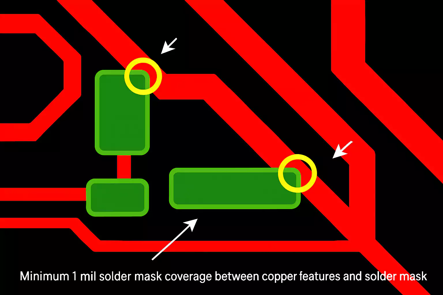
- Minimum Mask Web Width: Keep at least 4 mils between openings to avoid fragile slivers that may peel off.
- SMD vs. NSMD Pads:
- NSMD pads are generally preferred for better solder joint quality.
- SMD pads may be used for very fine-pitch or mechanically critical areas.
- Via Tenting and Plugging: Cover or fill vias under BGA components to avoid solder wicking and improve reliability.
- Registration Tolerance: Account for ±3 mils mask-to-copper misalignment in your design to avoid pad coverage issues.
- Design Tool Tips: Always define mask expansion rules in your CAD tool and run a DFM check before sending Gerber files.
Signal Integrity & High-Frequency Impact
Although the primary role of solder mask is protection, it can affect signal integrity in high-speed or high-frequency PCB designs.
- Dielectric Constant (Dk): Most solder mask materials have a Dk between 3.5–4.0, which slightly alters impedance when covering traces.
- Signal Loss: In high-frequency applications, solder mask can increase signal attenuation due to its dielectric properties.
- Impedance Variation: Covering microstrip or coplanar traces may lead to impedance mismatches and reflection.
Design Tips:
- Leave critical high-speed traces (e.g., differential pairs) unmasked if precise impedance is required.
- Include solder mask layers in simulation tools when modeling signal performance.
- For high-frequency PCBs, consider low-loss solder mask materials where available.
In most standard designs, the impact is minimal—but for GHz-level signals, solder mask choices can make a measurable difference.
Common Issues in Solder Mask Application
Solder mask plays a critical role in protecting copper traces and maintaining PCB performance, but when improperly applied or poorly designed, it can become a source of failure. Understanding common solder mask issues and how to prevent them is essential for ensuring long-term reliability of printed circuit boards.
Common Solder Mask Issues
Here are the most frequent defects seen in solder mask layers during manufacturing and operation:
1. Delamination or Peeling
- Cause: Poor surface preparation, low adhesion materials, or inadequate curing.
- Effect: The mask lifts from the substrate, exposing copper traces and risking oxidation or short circuits.
- Prevention: Ensure thorough cleaning before application and use appropriate thermal curing profiles.
2. Solder Bridging (Mask Misalignment)
- Cause: Misaligned mask openings or insufficient solder mask web between pads.
- Effect: Solder can flow between adjacent pads during reflow, causing electrical shorts.
- Prevention: Apply proper mask expansion values and respect minimum mask web/sliver widths, especially in dense BGA or QFN layouts.
3. Incomplete Curing
- Cause: Insufficient thermal or UV exposure during the final curing stage.
- Effect: The mask remains soft or sticky, reducing chemical and mechanical resistance.
- Prevention: Follow manufacturer-specified exposure and baking parameters.
4. Air Bubbles or Voids
- Cause: Entrapped air during coating or layering.
- Effect: Trapped voids can lead to localized weak spots or moisture ingress.
- Prevention: Use vacuum lamination or degassing steps during LPI mask processing.
5. Color Inconsistencies or Contamination
- Cause: Contaminated equipment, inconsistent ink mixing, or environmental factors.
- Effect: Aesthetic and optical inspection issues; may also indicate processing instability.
- Prevention: Maintain cleanrooms, controlled humidity, and consistent process parameters.
6. ECM (Electrochemical Migration)
- Cause: Contaminants or humidity penetrating weak spots in the solder mask.
- Effect: Unwanted conductive paths form between adjacent traces, leading to leakage or shorts.
- Prevention: Use high-insulation resistance materials and ensure the solder mask fully covers critical copper features.
FAQ: Solder Mask
Why is solder mask usually green?
Green provides excellent contrast for visual inspection and automated optical inspection (AOI). It also has stable processing characteristics and is widely available. Other colors are used, but green remains the industry standard.
Is solder mask necessary?
Yes, in most cases. It prevents solder bridging, protects copper from oxidation, and improves electrical insulation. While some prototypes may omit it, solder mask is essential for reliability in production boards.
What’s the difference between LPI and dry film solder mask?
· LPI (Liquid Photoimageable): Used in most modern PCBs; suitable for fine-pitch designs; cost-effective.
· Dry film: Thicker, used in certain rigid-flex or specialty boards. Less common today.
Does solder mask affect signal performance?
Yes, especially in high-speed or RF circuits. Its dielectric properties can slightly impact impedance and signal loss. For critical traces, designers may avoid solder mask or use low-loss materials.
Can damaged solder mask be repaired?
Minor damage can be fixed with manual reapplication or UV-curable materials. However, repairs may not fully restore reliability, especially in high-performance applications.
Conclusion
Solder mask is more than just a protective coating on a printed circuit board—it plays a critical role in ensuring the reliability, manufacturability, and performance of modern electronics. From preventing solder bridging and oxidation to enabling finer pitch designs and enhancing signal integrity, its importance cannot be overstated.
By understanding the different solder mask types (like LPI and dry film), selecting the right materials for your application, and following best practices for design—such as proper mask expansion and via coverage—you can significantly reduce the risk of defects and improve long-term reliability.
Whether you're designing high-frequency RF boards, consumer electronics, or automotive-grade PCBs, choosing the right solder mask strategy is essential. Always consult your PCB fabricator’s capabilities and match your design to your product’s end-use environment.