When designing compact, high-performance electronics, the QFN package (Quad Flat No-Lead) is one of the most common surface-mount IC packages you’ll encounter in component datasheets. Known for its small footprint, excellent electrical performance, and efficient thermal conductivity, the QFN is widely used in mobile devices, automotive systems, and RF applications where space and performance are critical.
This guide covers everything you need to know about the QFN package — including what it is, how it works, the different types (such as the QFN package with lid), how it compares to QFP, and step-by-step tips on how to solder a QFN package in both prototyping and production environments.
What Is a QFN Package?
The QFN (Quad Flat No-Lead) package is a compact, square-shaped IC package that features metal pads located on the bottom surface instead of traditional protruding leads. These bottom pads are designed to solder directly to copper pads on the PCB, enabling a low-profile, high-performance connection.
Most QFN packages also include a large central Exposed Pad (EP) — a key feature that enhances thermal dissipation and adds mechanical stability during assembly.
In technical documentation, QFN packages may also be referred to as MLF (Micro Lead Frame), DFN (Dual Flat No-Lead), or SON (Small Outline No-Lead). While the names vary, they all share the same design principle: a thin, molded body with electrical and thermal contacts that exit through the underside of the package.
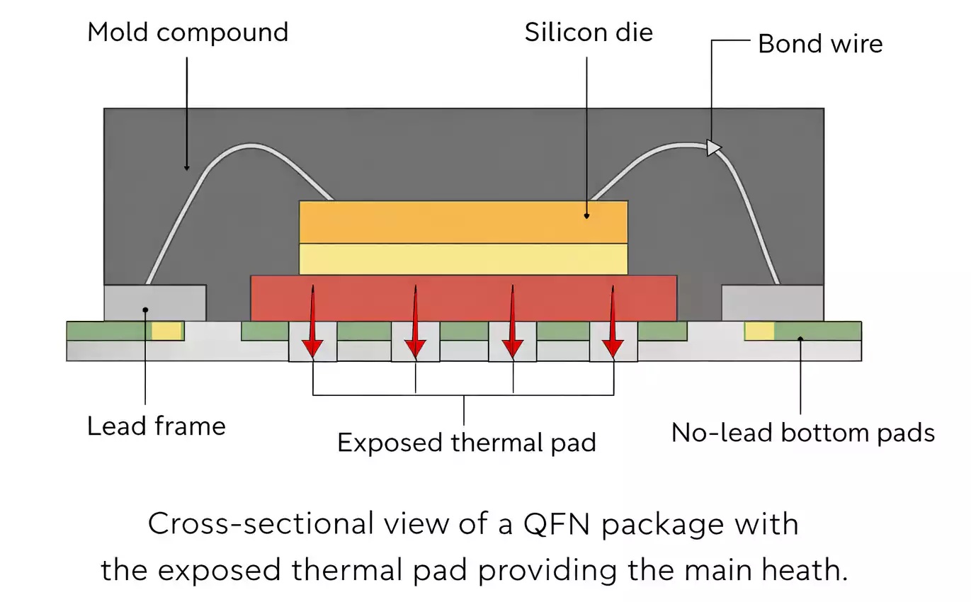
Inside the QFN Structure
Although the QFN looks simple from the outside, its internal structure combines several precise layers:
- Lead frame: the metal skeleton carrying electrical leads and providing thermal paths.
- Die: the actual silicon chip attached to the lead frame using epoxy or solder.
- Bond wires or flip-chip bumps: connect the die pads to the lead frame terminals.
- Mold compound: encapsulates and protects the die.
- Exposed Pad (EP): a large metal area on the bottom center that contacts the PCB for heat transfer.
In some high-frequency devices, the chip is connected via flip-chip technology, reducing wire length and improving signal integrity.
Why Engineers Choose QFN: Benefits and Limitations
Advantages
- Compact size and low profile: QFN packages are much thinner than traditional QFPs or SOICs.
- Excellent electrical performance: The short connection path reduces parasitic inductance and resistance.
- High thermal efficiency: The exposed pad provides a direct heat path to the PCB copper.
- Lower cost than BGA: It uses a simple lead frame instead of solder balls.
Limitations
- Hidden joints: All solder joints are underneath the device, so they cannot be visually inspected.
- Sensitive to solder process: Requires accurate stencil design and reflow temperature control.
- Difficult to rework: Removing and re-soldering a QFN without damaging nearby parts needs experience.
Despite these challenges, QFN remains the best compromise between size, cost, and performance for many modern electronics.
Common QFN Types and Variants
There are several variations of QFN, each optimized for different applications.
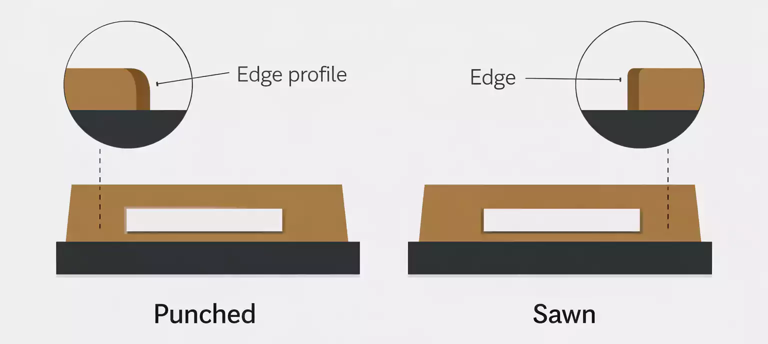
1. Punch vs. Sawn QFN
Early QFNs were separated from the panel using mechanical punching, leaving slightly rounded edges.
Modern production often uses saw singulation, producing cleaner, more accurate edges and smaller package tolerance.
Both function identically for PCB assembly.
2. Wettable-Flank QFN
A wettable-flank QFN has small plated sidewalls on each pad, allowing solder to climb up during reflow.
This creates visible fillets that can be detected by AOI (Automated Optical Inspection) systems — improving inspection capability without X-ray.
It is especially popular in automotive and high-reliability applications.
3. Thin and Very-Thin QFN (TQFN / VQFN)
When vertical height is critical, thin QFN versions are used.
They maintain electrical performance while reducing package thickness, ideal for smartphones and wearables.
4. QFN Package With Lid – Air-Cavity QFN
A QFN package with a lid is an air-cavity QFN, where the die is mounted in an open cavity and sealed with a lid rather than full plastic molding.
This design minimizes dielectric loading and enables the device to operate at very high frequencies.
Why add a lid?
- To protect sensitive MEMS or RF structures.
- To achieve hermetic sealing for high-reliability or aerospace systems.
- To allow post-assembly tuning or optical access before sealing.
Typical lid materials: metal, ceramic, or glass, bonded with epoxy or solder seal.
Air-cavity QFNs cost more but offer superior RF performance and heat resistance to molded types.
QFN vs. QFP: Which One to Choose?
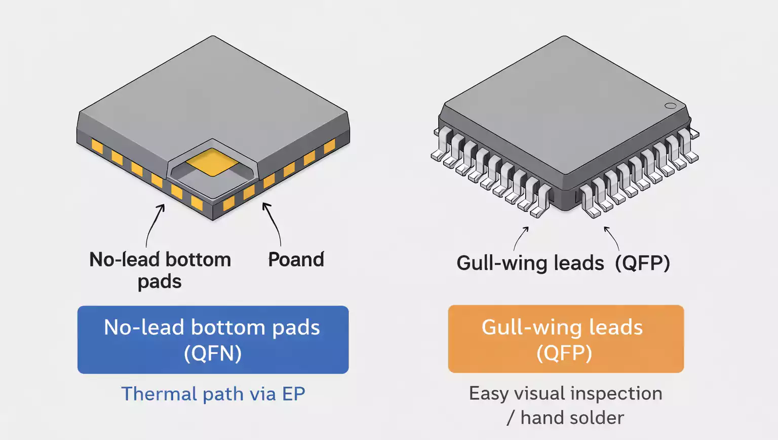
| Leads | No-lead, pads under package | Gull-wing leads visible on sides |
| Inspection | X-ray or AOI (wettable flank) | Easy visual inspection |
| Assembly | Requires precise stencil/reflow | Easier to hand solder |
| Thermal path | Direct EP to PCB | Limited heat transfer |
| Typical use | High-density, RF, thermal design | Prototypes, easy rework |
In short:
- Choose QFN when you need compact size, high speed, or strong thermal performance.
- Choose QFP when you prioritize ease of debugging, manual soldering, or visual inspection.
PCB Design Tips for QFN Packages
A successful QFN assembly depends largely on PCB footprint design.
Follow these practical guidelines:
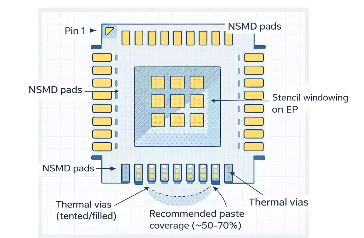
1. Land Pattern and Mask
Use the land pattern dimensions recommended in the component datasheet.
Typically, Non-Solder Mask Defined (NSMD) pads work better because they provide more reliable solder fillets.
Ensure a clear Pin-1 marking and adequate pad spacing to provide solder mask clearance.
2. Exposed Pad (EP) Layout
The EP must connect to a large copper area for heat dissipation.
You can also connect it to the ground plane through thermal vias — small plated holes that spread heat into internal layers.
If the vias are open, fill or tent them to avoid solder wicking during reflow.
3. Stencil Design
For the side pads, open the stencil normally.
For the center EP area, do not make a single large opening.
Instead, use multiple smaller “window-pane” apertures (for example, 50% total area coverage).
This controls solder volume, reduces floating, and minimizes voids.
4. Placement and Alignment
Because QFNs self-center during reflow, small placement errors are acceptable.
However, consistent solder paste printing is critical — uneven paste can cause tilt or open joints.
How to Solder a QFN Package
Knowing how to solder a QFN package correctly is essential for reliable performance.
There are two main methods: reflow oven (production) and hot-air tool (prototype or repair).
1. Reflow Soldering (Production)
- Apply solder paste through a laser-cut stencil.
- Place the QFN accurately using a pick-and-place machine.
- Run the reflow profile: preheat, soak, reflow, and cool down per solder paste specifications.
- Inspect joints using X-ray or AOI.
Pay special attention to the center pad — too little paste may cause poor thermal contact; too much may lift the component.
2. Hand Soldering / Hot-Air Method (Prototype)
When a reflow oven is unavailable, you can hand-solder QFN devices with care:
Tools needed: hot-air station, flux, fine tweezers, solder paste or preform, and magnification.
Steps:
- Apply a thin layer of solder paste to the PCB pads.
- Place the QFN carefully, aligning Pin-1.
- Heat gradually with hot air until solder reflows.
- Allow to cool and clean the flux residues.
- Check continuity and shorts with a multimeter.
Avoid overheating or moving the chip while molten.
For small-pitch QFNs, hand soldering is risky; use reflow whenever possible.
Inspection and Troubleshooting
Because QFN solder joints are hidden, inspection requires special methods.
1. AOI and X-ray
- AOI (Automated Optical Inspection): works only if wettable flanks are visible.
- X-ray inspection: the most reliable way to see solder joint shape and voids under the package.
2. Common Defects and Fixes
| Solder bridging | Excess paste, poor stencil design | Reduce paste, adjust stencil opening |
| Open circuit | Insufficient solder, misalignment | Verify paste coverage, improve placement accuracy |
| Device float / tilt | Too much EP solder | Reduce EP aperture area (50–70%) |
| Voids in EP | Poor reflow or trapped flux | Adjust temperature profile, window-pane stencil |
| Tombstoning / movement | Uneven heating or paste distribution | Balance paste volume and airflow |
Proper PCB design and stencil control can eliminate most of these issues.
Where QFN Packages Are Used
QFN packages appear across almost every electronics segment:
- Consumer electronics: smartphones, tablets, wearables.
- Automotive systems: sensors, controllers, infotainment.
- Communication and RF: Wi-Fi, Bluetooth, 5G front-end modules.
- Industrial and medical electronics: compact controllers and sensors.
Their combination of small size and high performance makes them ideal for next-generation designs.
Frequently Asked Questions (FAQ)
Is QFN the same as MLF or DFN?
Yes, they are similar “no-lead” packages. DFN usually refers to two-sided versions, while QFN has pads on all four sides.
What is a QFN package with lid used for?
It’s an air-cavity QFN sealed with a metal or ceramic lid, ideal for RF, MEMS, or hermetic applications where a standard plastic molded package is not sufficient.
Can I hand-solder a QFN package?
Yes, but only for prototypes. Use a hot-air station, solder paste, and flux carefully. For production, always use reflow.
Why is the exposed pad important?
It acts as the main heat path from the die to the PCB and often connects to ground. Poor soldering here leads to overheating.
Do I always need X-ray inspection for QFN?
Not always. Wettable-flank QFNs can be inspected optically, but standard QFNs generally need X-ray for quality assurance.
Summary
The QFN package offers a compact size, excellent signal integrity, and strong thermal performance — ideal for modern high-density designs.
Though assembly is more demanding, proper PCB layout, stencil design, and reflow control ensure reliable results in mass production.
For RF, MEMS, or hermetic applications, consider the QFN package with lid (air-cavity QFN) for enhanced shielding and reliability.
FastTurnPCB provides precision PCB fabrication and assembly services for QFN, BGA, and other fine-pitch components — from prototype to volume production.