


In modern electronics manufacturing, PCB panelization is a practical design step. Instead of producing and handling circuit boards one by one, multiple boards are combined into a single larger panel. This is called PCB panelization.

What Is a PCB Panel?
A PCB panel is a large sheet holding several smaller boards. These can be identical or mixed. The purpose is simple: make assembly faster, reduce handling, and lower production costs. During solder paste printing, pick-and-place, reflow soldering, AOI, and testing, machines can process the entire panel at once. After assembly, boards are separated using scoring, routing, or laser cutting.
Small or irregular-shaped boards almost always require panelization. Otherwise, they can’t travel smoothly through the production line or fit in stencils and conveyors.
Common PCB Panel Sizes and Usable Area
Most fabrication and assembly houses use a few standard panel sizes to match their machines and tooling. The most common panel sizes in the industry are:
- 24 × 18 inches
- 12 × 18 inches
- 24 × 9 inches
- 12 × 9 inches
These formats are compatible with most solder paste printers, pick-and-place systems, and reflow ovens.
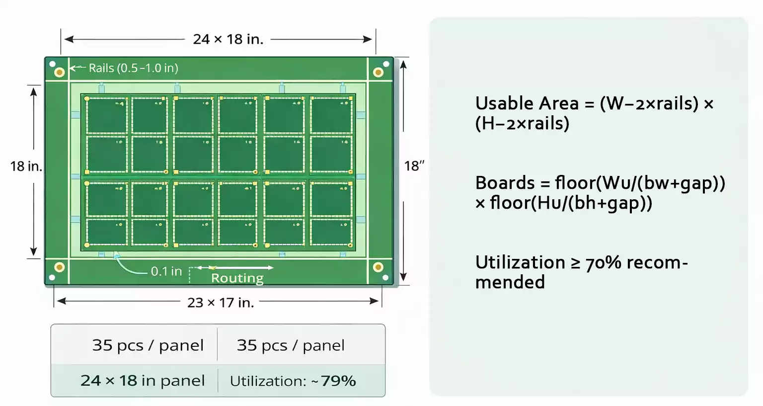
However, not all of that area is usable. Each panel includes rails (also called panel borders or process edges) that help with transportation and tooling. To calculate usable space:
- Subtract the rails from the outer panel size (usually on both sides).
- Reserve spacing between boards for routing or scoring.
- Arrange the boards in rows and columns.
- Aim for 70% or higher panel utilization to balance efficiency and manufacturability.
Example:
A 24 × 18-inch panel with 0.5-inch rails on all sides gives a working area of 23 × 17 inches. If each board is 3 × 3 inches with 0.1-inch spacing, you can fit roughly 7 × 5 boards, for a total of 35 boards per panel.
Rails, Fiducials, and Tooling Holes
Rails (Process Edges)
Rails are the solid edges around the panel that allow machines to grip and guide it. They provide extra stiffness and space for tooling holes and fiducial marks. The recommended width is at least 0.5 inch (12.7 mm) on each side. Complex or multilayer boards may use 1-inch rails for better support.
Fiducial Marks
Fiducials are small, round copper dots that help automated machines align the panel during assembly. Each panel should include at least three global fiducials, placed asymmetrically for correct orientation. Typical fiducial size is 1–3 mm in diameter, with at least 3–5 mm clearance from the panel edge or routing path.
Tooling Holes
Tooling holes are non-plated holes used for mechanical alignment in solder paste printing, wave soldering, or testing fixtures. They are usually 1.0–2.0 mm in diameter and located on the rails. Always keep tooling holes clear of traces and components.
Adding rails, fiducials, and tooling holes ensures smooth production and accurate alignment for stencil printing and pick-and-place machines.
V-Scoring vs. Tab Routing (Mouse Bites)
When the PCB panel is finished, the small boards must be separated. The two main depaneling methods are V-scoring and Tab (mouse-bite) routing.
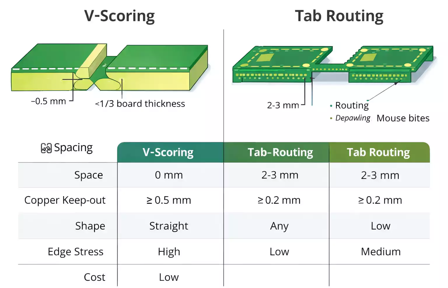
V-Scoring
V-scoring uses straight cutting lines (V-grooves) on both sides of the board. The grooves leave a thin “web” of material—typically about one-third of the board thickness—that can be easily snapped apart after assembly.
- Works only for straight lines that run from one edge to another.
- Best for rectangular boards and high-volume production.
- Boards are tightly spaced (0 mm gap).
- Requires copper clearance of ≥ 0.5 mm from the score line.
- Some manufacturers limit the number or angle of V-cuts. Excessive scoring can lead to panel warping or extra charges.
Tab Routing (Mouse Bites)
Tab routing connects boards with small bridges that include rows of tiny perforations (mouse bites). After assembly, these tabs are broken or routed off.
- Ideal for irregular shapes or boards with connectors near the edge.
- Supports curved or complex outlines.
- Requires routing channels of about 2.0 mm width.
- Copper clearance should be ≥ 0.2 mm from the routed edge.
- Leaves small burrs that can be sanded or milled off.
Spacing, Copper Keep-Out, and Component Clearance
Every depaneling process needs proper spacing and clearance to prevent damage:
| V-Score | 0 mm (shared line) | ≥ 0.5 mm | ≥ 1.0 mm |
| Tab / Routing | 2–3 mm channel | ≥ 0.2 mm | ≥ 1.0–2.0 mm |
| Laser Cutting | < 0.5 mm possible | ~0.1–0.2 mm | ≥ 0.2 mm |
Laser depaneling is gaining popularity because it leaves minimal stress and almost no debris. However, it’s more expensive and less common in standard volume production.
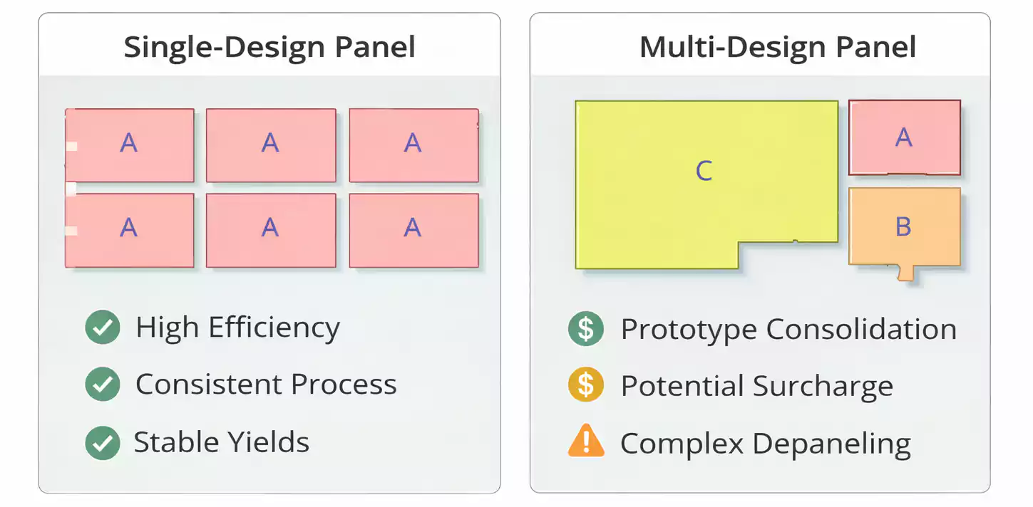
Single-Design vs. Multi-Design Panels
A single-design panel contains identical boards arranged in a grid. This is the most efficient and reliable setup for volume production—uniformity simplifies placement, testing, and yield control.
A multi-design panel (also called a mixed panel) includes multiple board designs in a single panel. It is popular for prototypes or small batch orders because it saves setup costs when multiple designs share the same process. However:
- Different outlines and component heights complicate depaneling.
- Panel utilization may drop.
- Many manufacturers charge extra for multi-design panels due to the additional CAM and routing work required.
For large orders, it’s almost always cheaper and safer to keep one design per panel.
Cost Factors: When Panelization Saves or Adds Cost
Panelization reduces cost by increasing machine efficiency. One stencil print-and-pick-and-place cycle processes many boards, minimizing handling loss.
To keep costs low:
- Use standard panel sizes (24×18 or 12×18 inches).
- Provide at least 0.5-inch rails for stable transport.
- Choose V-score for simple shapes and routing for complex ones.
- Keep all depaneling lines straight and continuous when possible.
- Include clear notes in your Gerber or fabrication drawing describing the panel type, cut method, and edge spacing.
DFM Checklist for PCB Panelization
Before submitting your files, review this simple checklist to ensure your design is DFM-ready:
- Include the full outline layer showing the panel border, V-cut, or routing lines.
- Specify the panelization method (V-score, tab, or both).
- Add rails (≥ 0.5 inch) on both sides of the panel.
- Define fiducials (3 global marks) and tooling holes on rails.
- Maintain copper clearance: 0.5 mm from V-cut or 0.2 mm from routing.
- Check component-to-edge distance: ≥1 mm (V-score) or ≥2 mm (routing).
- Label each board clearly for identification.
- Confirm maximum and minimum panel size with your manufacturer.
- State whether X-outs (defective boards left in the panel) are allowed.
Quick Reference Table
| Line Shape | Straight only | Any shape | Any shape |
| Spacing | 0 mm | 2–3 mm | <0.5 mm |
| Copper Clearance | ≥0.5 mm | ≥0.2 mm | ~0.1 mm |
| Edge Stress | Higher | Medium | Very low |
| Burr / Debris | None | Small burrs | None |
| Cost | Low | Medium | High |
| Best For | Rectangular boards | Irregular shapes | Fragile or dense designs |
FAQ
Do all small boards need panelization?
Yes, if a board is under 50 mm wide and unsuitable for automated equipment. Panelization provides stability for handling.
When should I add rails or process edges?
Always include rails if the panel will go through automatic assembly. They provide grip for the conveyor and space for fiducials and tooling holes.
What are standard panel sizes?
Most assembly lines support 24×18, 12×18, 24×9, and 12×9 inches. Always confirm the preferred size with your contract manufacturer.
How wide should rails be?
Typically, 0.5 inch is enough for most boards. For heavy or multilayer PCBs, increase to 1 inch.
V-Score or Tab? Which one is better?
V-score gives higher density and lower cost for rectangular boards. Tab routing is better for irregular shapes and delicate components near the edge.
Conclusion
Panelization may look like a small step, but it strongly affects manufacturability, yield, and total cost.
By starting with standard panel sizes, clear rails, correct spacing, and well-defined V-score or tab routing, you make life easier for your PCB fabricator and assembly line.
Always choose your depaneling method first, then adjust spacing, copper keep-out, and rails around it. That simple order will help you avoid costly redesigns or mechanical damage later.
For reliable, high-quality PCB fabrication and assembly—including professional panelization and quick-turn production—consider working with FastTurn PCB. Their engineering team can help you design the perfect panel layout for both small batches and high-volume runs.
