What does PCB stand for? PCB stands for Printed Circuit Board—a flat, laminated board found inside virtually every electronic device. It provides mechanical support for components and establishes electrical connections between them through patterned copper traces. From smartphones and laptops to automotive control units and industrial power supplies, PCBs form the backbone that makes modern electronics reliable, compact, and manufacturable at scale.
PCB at a Glance
- Full form: Printed Circuit Board
- Primary role: Mechanical support and electrical interconnection of electronic components
- Where you’ll find it: Consumer electronics, communications equipment, automotive systems, medical devices, industrial controllers, and more
- Not to be confused with:
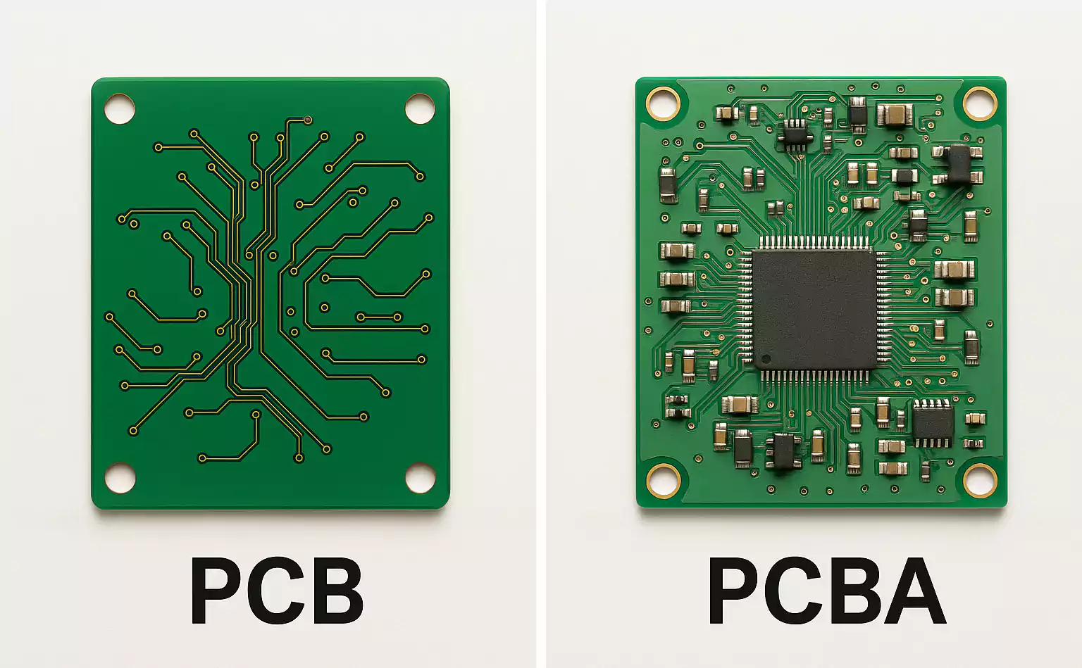
- PCBA (Printed Circuit Board Assembly): A PCB populated with electronic components
- PCB (Polychlorinated Biphenyls): A chemical compound unrelated to electronics
What a PCB Actually Does
Think of a PCB as the “city map” of a device. Copper traces act as roads, vias as tunnels between layers, pads as parking spots for components, and the board materials as the foundational infrastructure.
A well-designed PCB accomplishes three main goals:
- Electrical connectivity: Copper traces, plated through holes (vias), and pads create low-impedance, reliable paths between components, replacing bulky point-to-point wiring with precise, repeatable connections.
- Mechanical support: The board keeps components aligned and secured, whether in a handheld gadget or a car engine compartment, maintaining integrity even under vibration, shock, and temperature changes.
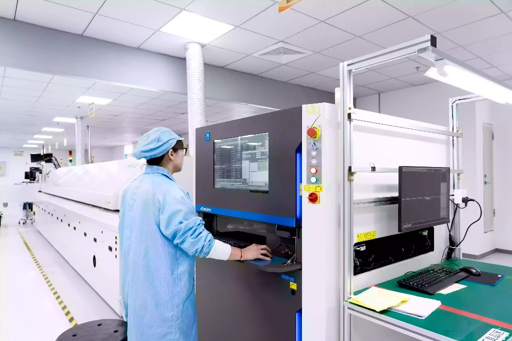
- Manufacturability and testability: PCBs are optimized for automated assembly (pick-and-place, reflow, wave soldering) and inspection (AOI, X-ray, ICT). Standardized footprints, solder mask openings, and test points help minimize defects and streamline production.
Inside a PCB: Layers, Materials, and Structure
A typical PCB is a laminated stack of copper and insulating (dielectric) materials. While specific builds vary, most boards include:
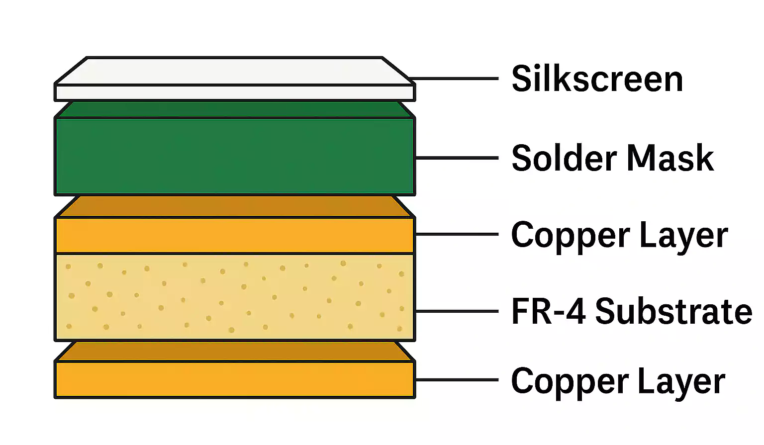
- Copper layers: Thin copper sheets etched into traces, planes, and pads. Outer layers carry component pads and routing; inner layers may host power/ground planes or extra routing.
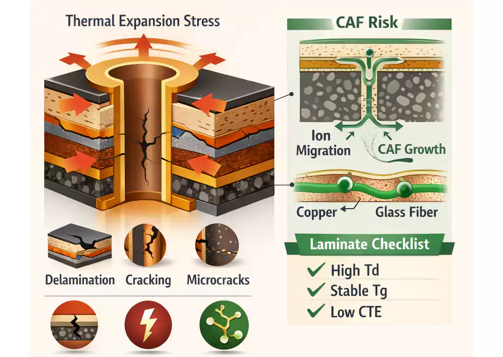
- Dielectric (substrate): Insulating material between copper layers. FR-4 (glass-reinforced epoxy) is standard; polyimide films are used for flexible boards; metal-core structures (aluminum or copper) help with heat management in high-power designs.
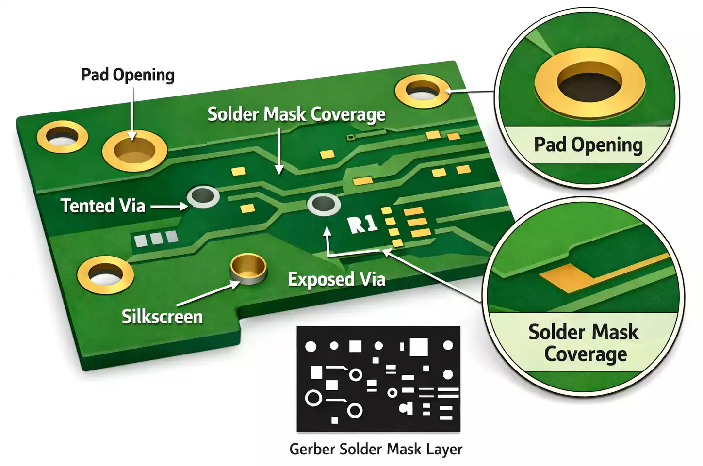
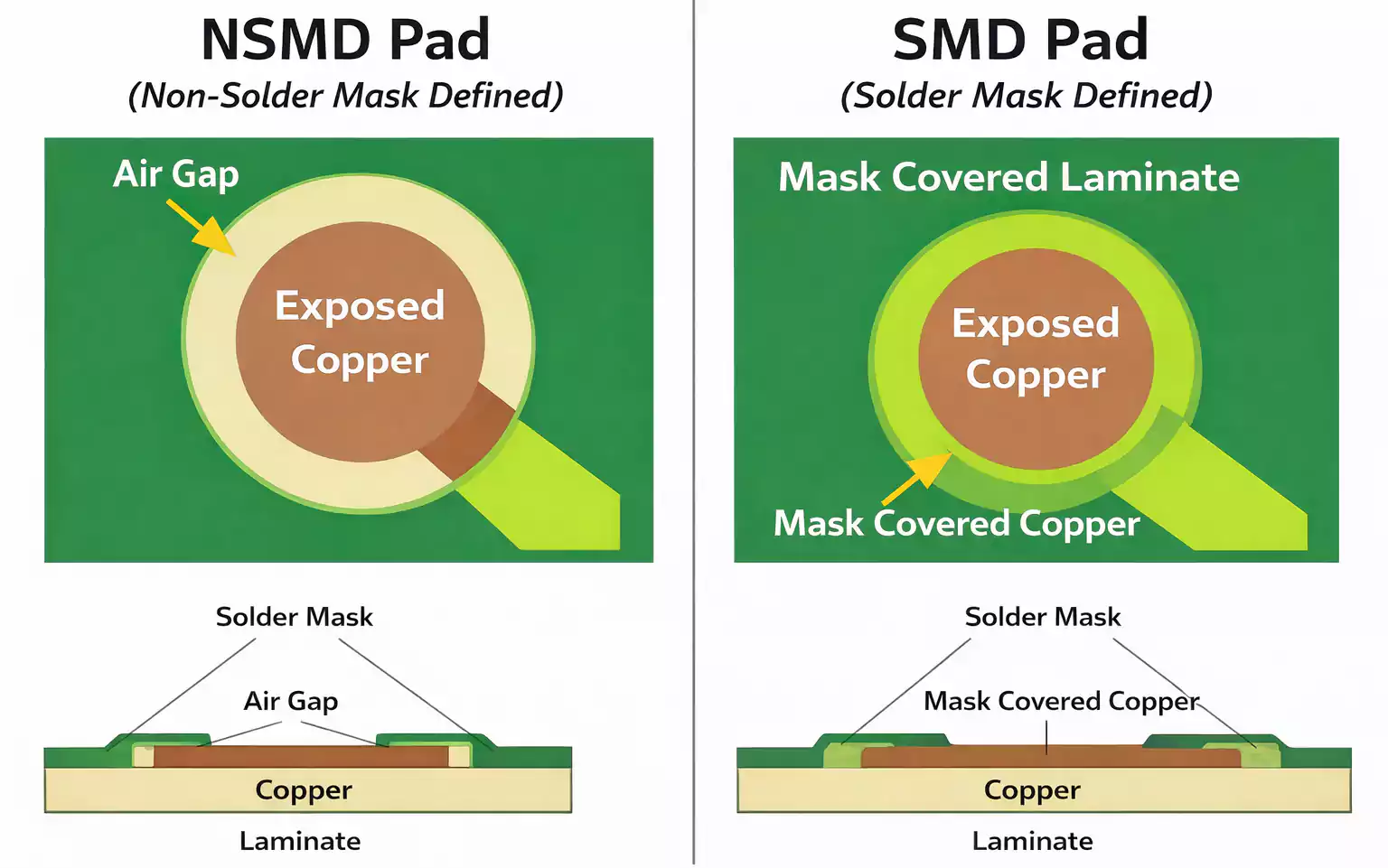
- Solder mask: The familiar green (or black, blue, red, white) coating insulates copper, exposing only the pads to be soldered. It prevents solder bridges and enhances reliability.
- Silkscreen (legend): Printed markings for reference designators, polarity, logos, and assembly notes.
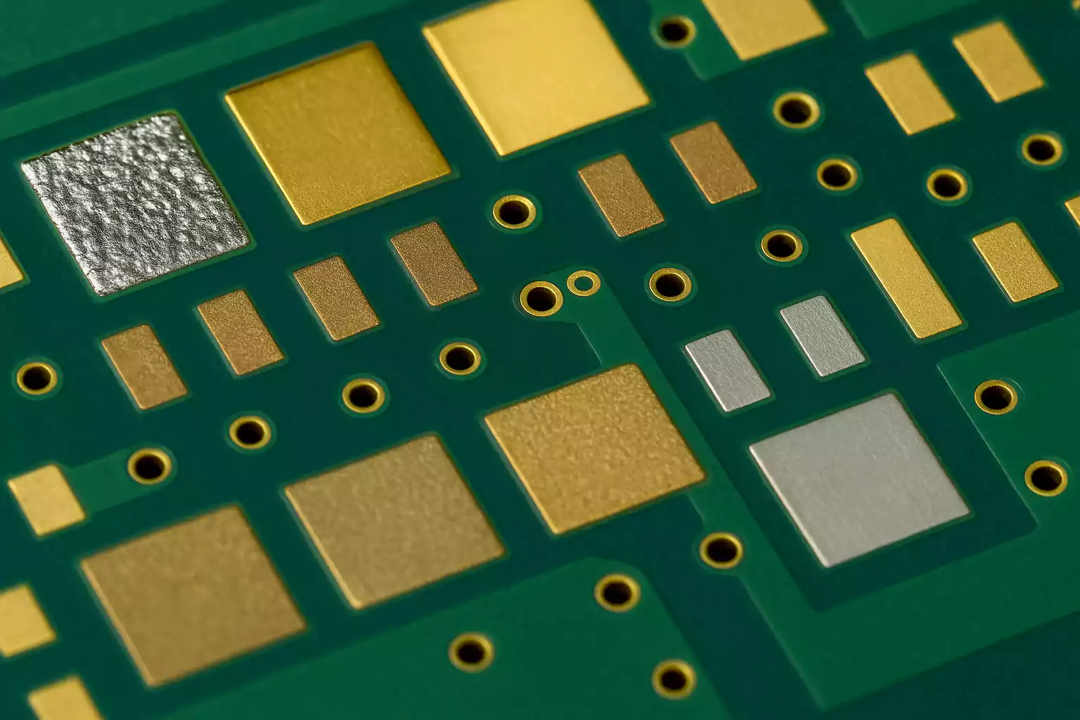
- Surface finish: A protective, solderable coating on exposed copper pads—options include ENIG (Electroless Nickel Immersion Gold), HASL (Hot Air Solder Leveling), OSP, and ENEPIG for fine-pitch or wire bonding needs.
Copper thickness is typically specified in ounces per square foot (oz/ft²). Standard designs use 1 oz (~35 µm) copper; high-current or rugged boards may require up to 2–4 oz or localized copper "coins" for better thermal and current handling.
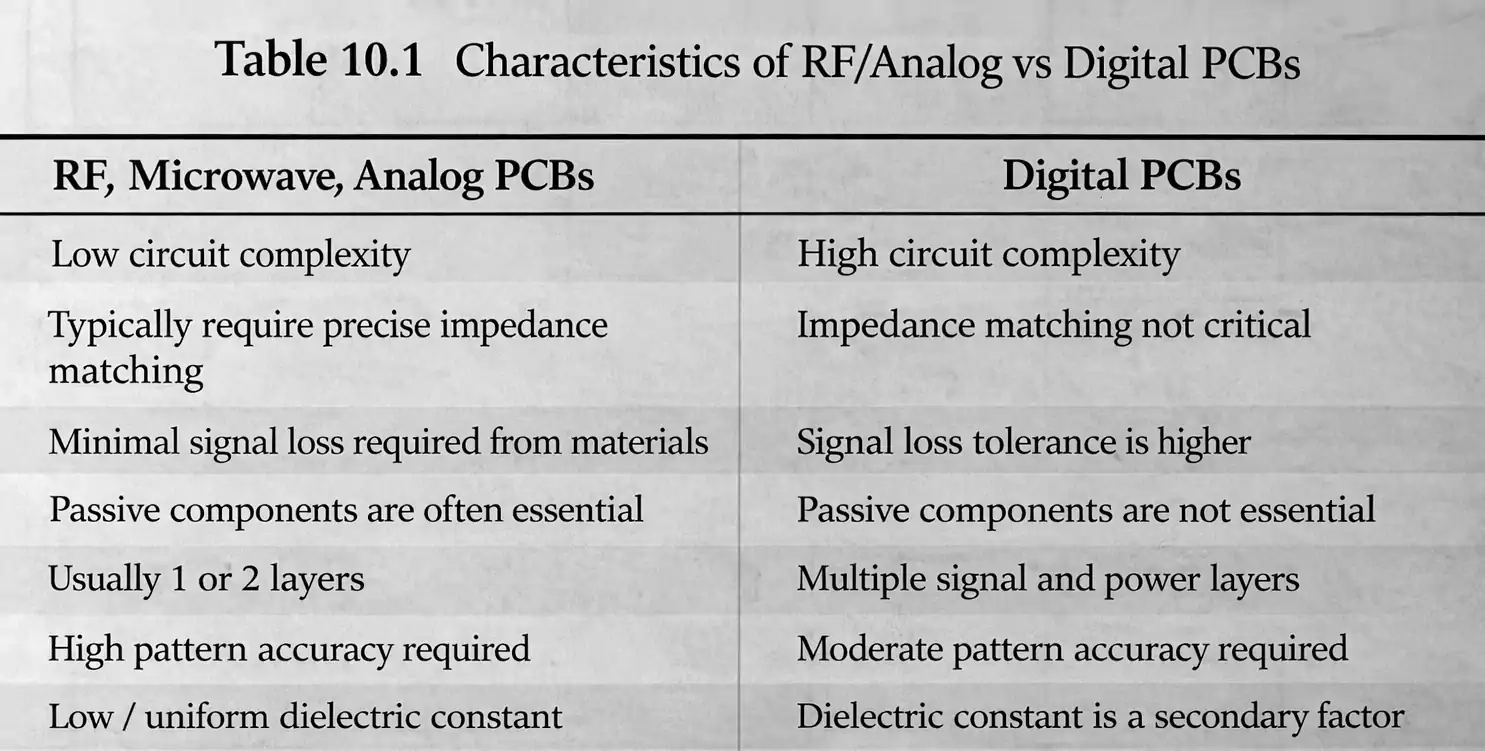
Common PCB Types
- Single-sided: One copper layer on one side. Simple and low cost, but limited in routing density.
- Double-sided: Copper on both sides with plated vias. The mainstream choice for most products.
- Multilayer: Four or more layers, often with internal power/ground planes for lower noise and EMI control. Many modern devices use 6, 8, or more layers.
- HDI (High-Density Interconnect): Uses microvias, blind/buried vias, fine traces, and thin dielectrics to maximize functionality in minimal space—common in smartphones and wearables.
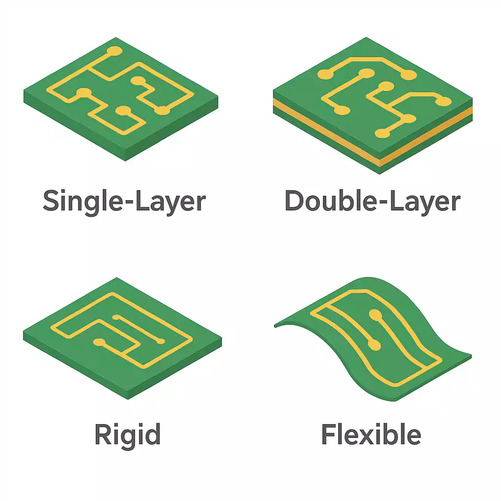
Rigid, Flex, and Rigid-Flex:
- Rigid: Standard FR-4 materials, offering durability and cost-effectiveness.
- Flex: Polyimide films allow the board to bend, ideal for tight spaces or dynamic applications.
- Rigid-flex: Combines rigid sections for component density with flexible tails for connectors, enabling complex three-dimensional assemblies.
PCB vs. PCBA: Understanding the Difference
- PCB (Printed Circuit Board): The bare board, with copper traces, vias, solder mask, and surface finish—no components attached, and not functional on its own.
- PCBA (Printed Circuit Board Assembly): The populated board, with components soldered onto the PCB using SMT (surface-mount technology), through-hole, or mixed processes. The PCBA is what actually powers your device.
Where You’ll Find PCBs
- Consumer electronics: Phones, laptops, wearables, gaming consoles, and smart home devices—where small size, high density, and cost control are essential.
- Automotive: Lighting, infotainment, power management, motor control, and advanced driver-assistance systems (ADAS). Materials must withstand high temperatures, vibration, and long service life.
- Industrial and power electronics: Motor drives, inverters, power supplies, PLCs, and sensors. Often require thicker copper, greater clearances, and robust insulation.
- Communications and computing: Routers, servers, base stations, and high-speed interconnects, where impedance control, low loss, and EMI performance are critical.
- Medical and aerospace: Patient monitors, imaging systems, avionics modules—where reliability, traceability, and regulatory compliance dictate material and process choices.
PCB Manufacturing in 8 Simple Steps
Here’s how a PCB is made, from digital files to a tested product:
- Data preparation: CAM engineers process Gerber/ODB++ files, stack-up, drill charts, and design rules. Panelization and DFM checks optimize yield and throughput.
- Inner-layer imaging & etching (multilayers): Circuits are transferred onto copper foils via photoimaging; unwanted copper is chemically etched away, leaving inner traces and planes.
- Lamination: Layers are stacked with prepregs and cores, then pressed under heat and pressure to form a solid laminate.
- Drilling & metallization: CNC or laser drills create vias and holes, which are then plated to form conductive barrels interconnecting layers.
- Outer-layer imaging & etching: Outer copper layers are patterned and etched to form final traces, pads, and planes.
- Solder mask & legend: The mask is applied, imaged, and cured; silkscreen legends print reference designators and markings.
- Surface finish: ENIG, HASL, OSP, or ENEPIG is applied to protect copper and ensure solderability.
- Electrical test & routing: Flying-probe or bed-of-nails testing checks for opens and shorts. Boards are routed (milled) or punched from the panel, inspected, and packed for shipment.
The assembly (PCBA) process then adds solder paste, components (placed by pick-and-place machines), reflow (SMT) or wave soldering (through-hole), and final inspection/testing.
A Quick Note on “PCB” vs. PCB (the Chemical)
In electronics, PCB always means Printed Circuit Board. In environmental or health contexts, PCB can also refer to polychlorinated biphenyls, industrial chemicals banned due to health risks. These are unrelated. When searching online, specify “electronics,” “board,” or “PCBA” to avoid confusion.
Essential Terms for Beginners
- PWB (Printed Wiring Board): Focuses on wiring/traces; often used interchangeably with PCB.
- Gerber files: The standard file set defining copper layers, solder mask, silkscreen, drill data, and board outline for manufacturing.
- Via: A plated hole connecting copper layers; types include through-hole, blind, buried, and microvia.
- Solder mask: The protective coating preventing solder bridging and shielding copper from oxidation.
- ENIG / HASL / OSP / ENEPIG: Common surface finishes balancing cost, shelf life, flatness, and solderability.
- Stack-up: The specified order and thickness of copper and dielectric layers, controlling impedance, EMI, and thermal characteristics.
Key Design Considerations
Even entry-level projects benefit from these fundamentals:
- Impedance control: For high-speed signals (USB, HDMI, PCIe, DDR), trace width, spacing, dielectric thickness, and copper weight must be optimized for target impedances (typically 50 Ω single-ended, 90–100 Ω differential).
- Thermal management: Power-dense components like regulators, FETs, and LEDs need copper pours, thermal vias, or even metal-core substrates to dissipate heat effectively.
- Clearance and creepage: High-voltage or high-power designs require adequate spacing to prevent arcing and ensure safety.
- DFM/DFA: Designing for manufacturability and assembly reduces costs and defects. Standardize footprints, avoid unnecessary microvias, and follow your fabricator’s minimums for trace/space, via sizes, and annular rings.
- Testability: Include test pads for power rails and key nets—this makes bring-up and production much easier.
Frequently Asked Questions
1. What does “PCB” stand for in electronics?
Printed Circuit Board—the laminated substrate with copper patterns that interconnect and support your device’s components.
2. Is a PCB the same as a PCBA?
No. A PCB is the bare board; a PCBA has all components mounted and soldered.
3. Why do I see “PCB” as a chemical term online?
That refers to polychlorinated biphenyls, an industrial chemical unrelated to electronics. Add “electronics,” “board,” or “PCBA” to your search for clarity.
4. What are the most common PCB materials?
FR-4 for general use, polyimide for flex boards, and metal-core (aluminum or copper) for high-power or LED applications.
5. Where are PCBs used?
Virtually everywhere: consumer electronics, servers, telecom equipment, EVs, factory automation, medical devices, and aerospace modules.
6. Which surface finish should I pick?
For general SMT: ENIG offers flat pads and good shelf life; lead-free HASL is economical; OSP is low-cost for fine-pitch but needs careful handling; ENEPIG is ideal for gold wire bonding and mixed-tech assemblies.
7. Do I need an HDI board?
Choose HDI for extremely fine-pitch components, short interconnects, or strict space constraints. Otherwise, a well-designed multilayer stack-up may be sufficient.

Summary
A PCB—Printed Circuit Board—is the essential platform that brings electronic designs to life. If you’ve ever wondered what does PCB stand for, it refers to the board that provides mechanical support and precise copper interconnections for electronic components. This combination delivers the performance, reliability, and compact size modern devices require.
By understanding PCB fundamentals—including board structure and materials, common types (rigid, flex, multilayer, HDI), the difference between PCB and PCBA, and key manufacturing and design principles—you can plan more effectively, reduce costly revisions, and collaborate better with suppliers. Whether you're prototyping a new device or scaling production, mastering these essentials is the foundation for building robust, high‑quality, and manufacturable electronics.