


Introduction
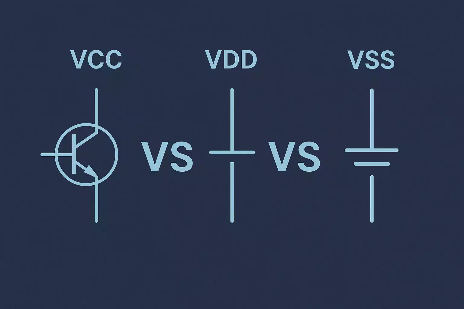
VCC, VDD, and VSS are common power supply labels found in electronic circuits. Although they look similar, each has a different meaning and comes from a specific type of transistor technology. VCC is often used with bipolar junction transistors (BJTs), while VDD and VSS are related to field-effect transistors (FETs), such as MOSFETs.
VCC and VDD often refer to the same voltage in modern circuits, which can lead to confusion across components and datasheets.
This article defines VCC, VDD, and VSS, explores their origins and usage, and provides practical labeling guidelines. Related terms like VEE and GND are also discussed.
Terminology and Definitions
VCC (Voltage at the Collector)
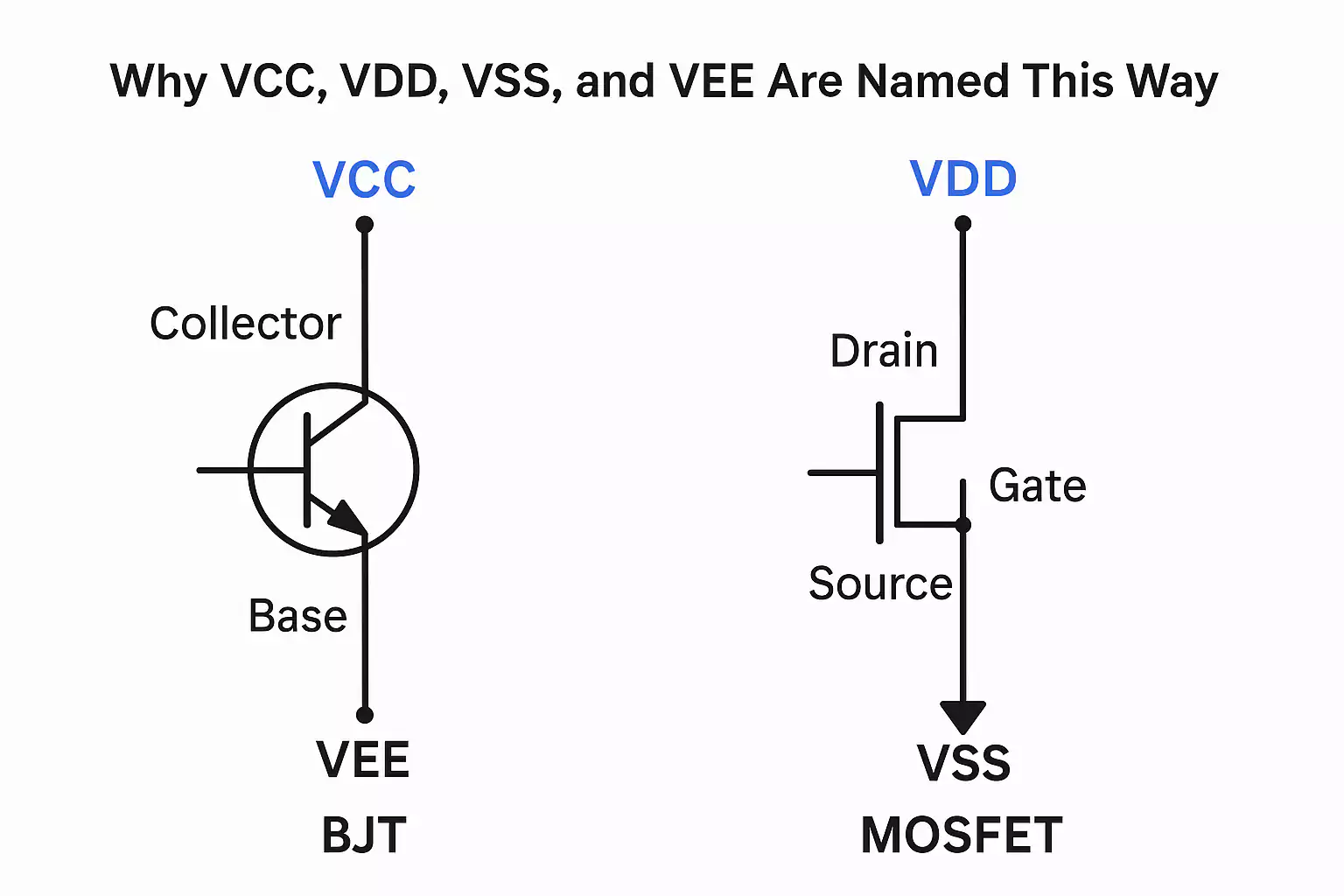
VCC stands for "Voltage at the Collector" and originates from bipolar junction transistor (BJT) technology. In a BJT circuit, the collector is the terminal where the main current flows from the power supply into the transistor. VCC typically refers to the positive supply voltage connected to the collector of an NPN transistor.
In most digital logic circuits, especially those using TTL (Transistor-Transistor Logic), VCC is commonly used to label the main positive voltage rail—such as +5V or +3.3V.
VDD (Voltage at the Drain)
VDD means "Voltage at the Drain" and is used in circuits based on field-effect transistors (FETs), particularly MOSFETs. In these devices, the drain is the terminal where current flows out of the transistor. VDD refers to the positive supply voltage connected to the drain of an N-channel MOSFET.
VDD is widely used in CMOS (Complementary Metal-Oxide-Semiconductor) technology. In many modern integrated circuits, VDD refers to the main positive power rail, even if the internal circuit no longer directly follows the original drain-structure logic.
VSS (Voltage at the Source)
VSS stands for "Voltage at the Source" and also comes from MOSFET-based technology. It refers to the ground or 0V reference point in the circuit, usually connected to the source terminal of an N-channel FET.
In digital ICs, especially CMOS designs, VSS is often used in place of "GND" to label the ground connection.
VEE (Voltage at the Emitter)
VEE is a term related to BJT circuits, specifically indicating the negative voltage supply connected to the emitter of a PNP transistor or to the emitter in circuits using a dual supply (positive and negative rails). It is commonly seen in analog designs, such as operational amplifiers, where negative voltage rails are required.
Summary Table
| Label | Meaning | Origin Technology | Typical Role | Common Voltage |
|---|---|---|---|---|
| VCC | Voltage at Collector | BJT | Positive supply rail | +5V, +3.3V |
| VDD | Voltage at Drain | MOSFET / CMOS | Positive supply rail | +3.3V, +1.8V |
| VSS | Voltage at Source | MOSFET / CMOS | Ground or 0V | 0V |
| VEE | Voltage at Emitter | BJT | Negative supply rail | –5V, –12V |
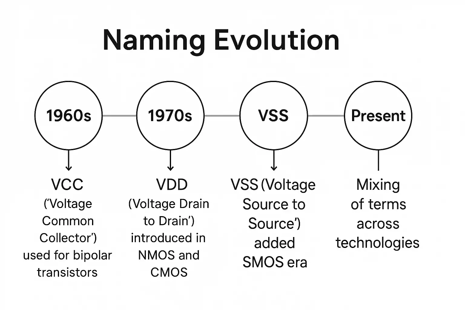
Naming History and Standard Origins
From BJT to MOSFET: The Source of VCC and VDD
The terms VCC and VDD come from different types of transistors used in electronic circuits. VCC was introduced with bipolar junction transistors (BJTs), where the collector terminal connects to the main positive supply. In contrast, VDD was created for MOSFETs, where the drain terminal connects to the positive supply. The different letters—C for collector, D for drain—reflect these hardware structures.
Evolution Through Logic Families
As logic families evolved—from TTL (which used BJTs) to CMOS (based on MOSFETs)—the naming conventions also changed. Early TTL ICs commonly used VCC and VEE to label the positive and negative supplies. When CMOS became widespread, VDD and VSS were adopted instead. These terms helped distinguish the supply rails based on the transistor type inside the chip.
IEEE and Industry Standards
While there is no universal enforcement of these labels, IEEE documentation and manufacturer datasheets have historically supported these naming practices. Some early standards from the 1960s and 1970s referenced voltage labels based on transistor terminal names to reduce confusion. However, as mixed-signal and BiCMOS technologies emerged, strict naming became harder to maintain.
Real-World Usage and Informal Practices
Today, the use of VCC, VDD, and VSS often depends on the manufacturer, chip architecture, or engineering culture.Similarly, VSS and GND are often treated as synonyms, even though VSS originally referred to the source terminal of a MOSFET.
Modern Usage and Practical Implications of Label Overlap
Labels Are No Longer Strictly Tied to Transistor Type
In today's electronics, the labels VCC, VDD, and VSS are often used interchangeably, regardless of the underlying transistor technology. While these terms originally referred to specific terminals—collector, drain, or source—modern integrated circuits may use any label based on company tradition or design conventions. For example, a CMOS microcontroller might still use VCC to refer to its main power rail, even though there is no collector involved.
Common Examples of Mixed Usage
Many microcontrollers, FPGAs, and digital ICs use VCC to indicate the main supply voltage, even when internally built on CMOS.For instance:
- AVR microcontrollers often use VCC and GND
- ARM-based chips may use VDD, VSS, or even multiple rails like VDDIO and VDDA
- Some ICs from different manufacturers use VDD and GND, while others use VCC and VSS for similar functions
Multi-Voltage and Mixed-Technology Systems
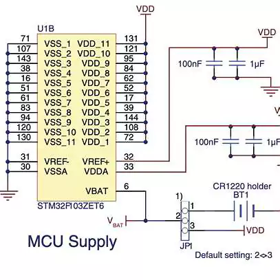
Modern designs often include multiple voltage domains, such as 1.2V core, 1.8V I/O, and 3.3V analog supplies. These are labeled with variations like VDDIO, VDDA, or even VCCINT, depending on function. This complexity makes clear labeling essential for debugging and integration, especially in mixed-signal or BiCMOS systems where both BJT and FET devices may coexist.
Design Risks of Label Confusion
Assuming that VCC and VDD are always interchangeable can lead to serious design errors. For example, connecting a 5V VCC to a pin labeled VDD on a 3.3V-only IC may damage the component. Similarly, misinterpreting VSS as GND without confirming actual pin behavior can affect performance in sensitive analog systems.
Proper labeling and reading of schematics, pinouts, and datasheets are critical, especially when dealing with level shifters, power management ICs, or devices with isolated grounds.
Comparison Table and Summary Overview
To clearly understand the differences between VCC, VDD, VSS, and VEE, the table below summarizes their origin, meaning, and typical usage in electronic circuits:
Power Label Comparison Table
| Label | Full Meaning | Origin Technology | Typical Role | Common Voltage Levels | Also Seen As |
|---|---|---|---|---|---|
| VCC | Voltage at Collector | BJT | Positive power supply | +5V, +3.3V | V+, VDD (in CMOS) |
| VDD | Voltage at Drain | MOSFET / CMOS | Positive power supply | +1.8V, +3.3V, +5V | VCC (in practice) |
| VSS | Voltage at Source | MOSFET / CMOS | Ground / 0V reference | 0V | GND, DGND, AGND |
| VEE | Voltage at Emitter | BJT | Negative power supply | –5V, –12V | V–, NEG, –Vcc |
Practical Tips and Use Cases
1. Read the Datasheet First
Always refer to the component's datasheet before connecting power. Label meanings like VCC or VDD may vary by manufacturer or device family.
2. Use Descriptive Net Labels in Schematics
In complex designs, label power nets clearly (e.g., VDD_3V3, VSS_ANA, VCCINT) to avoid confusion between voltage domains.
3. Keep Labels Consistent
When designing multi-board or collaborative systems, choose a consistent naming convention across all schematics and documentation.
4. Separate Analog and Digital Grounds
In mixed-signal designs, use labels like AGND (Analog Ground) and DGND (Digital Ground) instead of a generic VSS to avoid signal noise.
5. Avoid Assumptions in Multi-Supply Systems
In systems with multiple power rails (e.g., 1.2V, 1.8V, 3.3V), don't assume VDD always refers to the same voltage. Use context-aware labels.
6. Check for Inverted Logic
In some analog or negative-voltage systems, VEE may be a negative supply. Ensure proper orientation to prevent device damage.
Frequently Asked Questions (FAQ)
Is VCC the same as VDD?
Not always. VCC is traditionally used for BJT-based circuits, while VDD comes from MOSFET-based designs. In modern systems, both often refer to the positive supply voltage, but the choice of label depends on the component and manufacturer.
Can VSS be used instead of GND?
Yes, in most cases. VSS is the ground reference in MOSFET/CMOS circuits and is typically equivalent to GND (0V). However, some systems may use multiple grounds (e.g., analog and digital), so it's important to verify the context.
What does VEE mean, and when is it used?
VEE refers to the negative supply voltage in BJT-based or analog circuits, such as operational amplifiers. It's often seen in dual-supply systems (e.g., ±12V) and represents the voltage connected to the emitter of a transistor.
Why do some CMOS chips use VCC instead of VDD?
This is mostly due to legacy labeling or manufacturer preference. Even though CMOS circuits use FETs, some vendors continue using VCC for familiarity.
What happens if I connect 5V to a VDD pin rated for 3.3V?
Doing so can damage the component. VDD defines the expected supply voltage level. Exceeding it may lead to overheating, latch-up, or permanent failure.
How do I label power nets in a multi-voltage system?
Use clear, specific labels like VDD_1V2, VDDIO, VSS_ANA or VCC3V3. This avoids confusion and helps identify voltage domains during design, testing, and troubleshooting.
Conclusion
VCC, VDD, VSS, and VEE originated from specific transistor types but are now often used by convention. Following datasheets and using consistent labeling helps prevent errors in modern circuit design.