Introduction
PCB lamination is a critical fabrication step where multiple layers of copper foil and dielectric materials are compressed and thermally bonded to form a cohesive multilayer circuit board. This process not only enables high-density interconnects and compact layouts but also plays a vital role in maintaining structural integrity and electrical performance under operational stress.
When lamination is improperly controlled—due to factors such as incorrect temperature profiles, material mismatch, or moisture contamination—it can result in serious reliability issues, including delamination, resin voids, and layer misregistration. These defects compromise both signal integrity and mechanical stability, potentially leading to premature board failure.
This article provides a comprehensive look at the PCB lamination process, covering everything from material selection and layer stack-up to thermal cycle management and defect prevention strategies—equipping designers and manufacturers with the insights needed to optimize multilayer PCB reliability.
PCB Lamination Basics
PCB lamination is the process of bonding multiple layers of copper and insulating dielectric materials into a single, unified circuit board. This process is essential for creating multilayer PCBs, which are widely used in complex electronics where surface space is limited and high-speed signal routing is required.
What Is PCB Lamination?
In its simplest form, PCB lamination involves stacking alternating layers of copper foil and prepreg (a resin-impregnated fiberglass material), then applying heat and pressure to fuse them into a solid board. The result is a strong, compact structure that maintains electrical connectivity and mechanical durability across all layers.
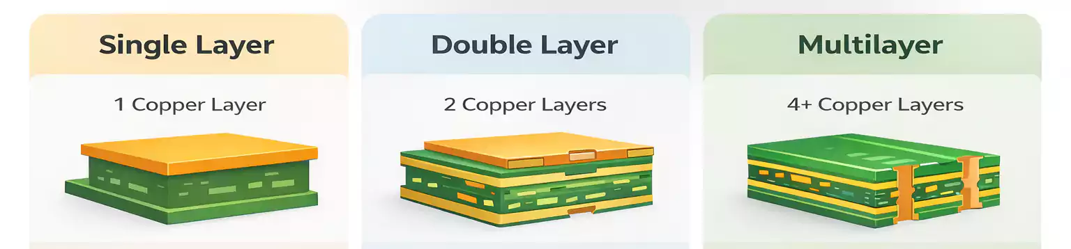
There are two primary lamination types used in PCB manufacturing:
- Standard (One-Time) Lamination
This is the most common process, where all layers are pressed and bonded in a single lamination cycle. It’s ideal for simple to moderately complex boards where blind or buried vias are not required. - Sequential Lamination
For advanced HDI (High-Density Interconnect) boards, sequential lamination is used. In this method, subsets of layers are laminated separately, drilled or imaged, then re-laminated with additional layers. This enables the creation of stacked vias, buried connections, and highly dense signal routing needed in next-gen devices.
Why Lamination Is Critical in PCB Fabrication
Lamination does more than just hold the board together—it directly impacts:
- Electrical performance: Proper bonding ensures low signal loss and impedance control.
- Reliability: Well-laminated boards resist thermal cycling, humidity, and mechanical stress.
- Manufacturability: Uniform lamination simplifies drilling, plating, and routing in later stages.
Failing to achieve good lamination can lead to issues like delamination, warping, internal shorts, or open circuits, all of which compromise product performance and lifespan.
As device complexity and layer count increase, mastering the fundamentals of PCB lamination becomes essential for engineers and manufacturers alike.
Materials and Key Parameters in PCB Lamination
The success of the PCB lamination process hinges on selecting the right materials and understanding their physical and electrical properties. These materials not only determine the board's structural integrity but also influence thermal behavior, signal performance, and long-term reliability—especially in high-frequency or high-density applications.
Core Lamination Materials
- Prepreg (Pre-impregnated Composite Resin)
- Prepreg is a fiberglass material pre-coated with partially cured resin. During lamination, it melts, flows, and fully cures to bond copper layers together.
- Available in different resin content and thicknesses (e.g., 106, 1080, 2116, 7628 glass styles) to meet specific stack-up and dielectric requirements.
- Core Material
- A rigid layer made of cured fiberglass and resin, often with copper foil on both sides.
- Serves as the foundation for the multilayer build-up and is often used in inner layers.
- Copper Foil
- Conductive layers etched to form circuit traces.
- Available in different weights (e.g., 0.5 oz, 1 oz, 2 oz) depending on current-carrying requirements and signal performance.
- Adhesive Films or Bonding Sheets (in specialty applications)
- Used for flexible or rigid-flex boards where traditional prepregs aren't applicable.
Critical Material Properties to Consider
| Parameter | Description | Why It Matters |
|---|---|---|
| Tg (Glass Transition Temperature) | Temperature at which resin transitions from rigid to rubbery state. | Higher Tg improves thermal stability and prevents delamination during reflow. |
| CTE (Coefficient of Thermal Expansion) | Rate at which material expands with temperature. | Lower CTE minimizes mechanical stress and via cracking under thermal cycling. |
| Dielectric Constant (Dk or Er) | Indicates how much a material slows down electrical signals. | Affects impedance and signal propagation, critical for high-speed designs. |
| Dissipation Factor (Df or Tan δ) | Measures dielectric loss or signal attenuation. | Lower Df ensures minimal signal loss, especially important in RF and microwave PCBs. |
| Moisture Absorption | Tendency of material to absorb water from the environment. | High absorption can lead to delamination, CAF (Conductive Anodic Filamenting), or dielectric failure. |
| Resin Flow and Gel Time | Determines how resin behaves during lamination (melting and curing). | Impacts void formation and bond strength between layers. |
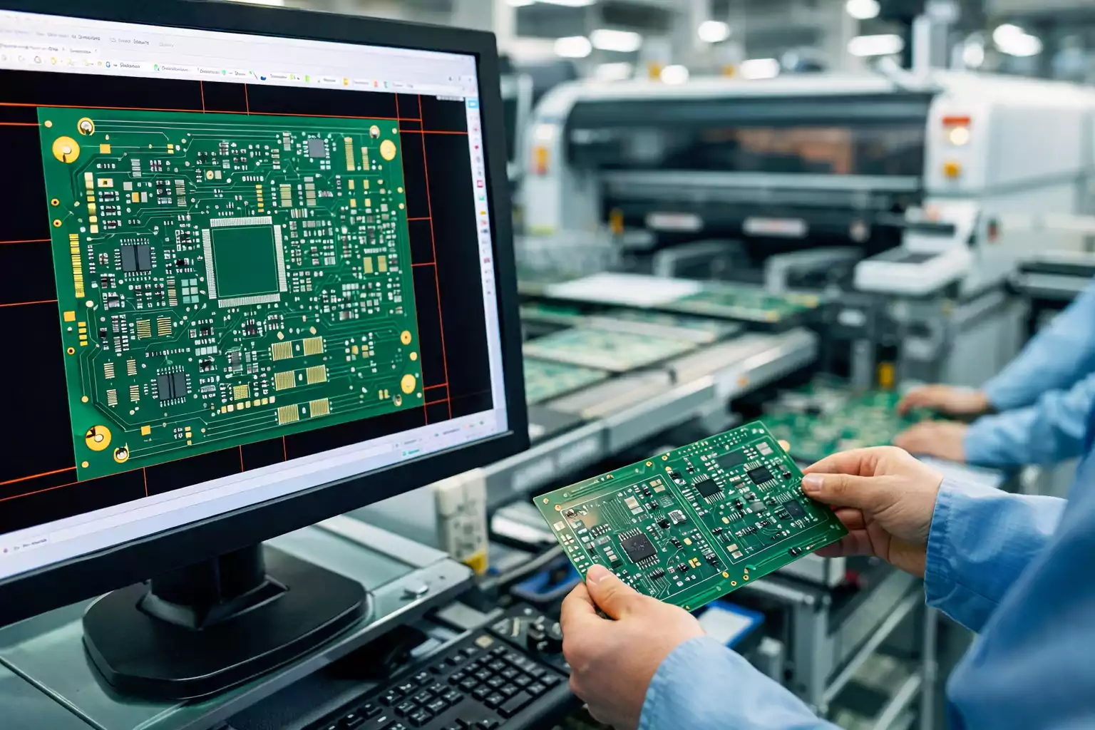
Detailed Lamination Process: How Multilayer PCBs Are Bonded
The lamination process is at the heart of multilayer PCB fabrication. It transforms individual copper layers, prepreg sheets, and core materials into a single, unified board with precise layer alignment, strong interlayer adhesion, and excellent electrical performance.
Understanding each stage of the lamination cycle is crucial to achieving reliable, high-quality multilayer PCBs—especially in high-speed, high-reliability applications.
Step 1: Inner Layer Preparation
Before lamination begins, inner copper layers are fabricated via imaging and etching processes. These layers form the circuit traces that will be electrically connected through vias.
- Cleaning & Oxide Treatment
Inner layers are chemically cleaned and treated with an oxide (or oxide alternative) layer to promote adhesion with the prepreg during lamination. - Layer Inspection
Automated Optical Inspection (AOI) ensures all patterns are free from shorts or opens before entering the lamination stage.
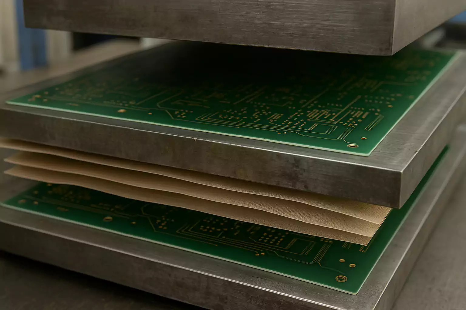
Step 2: Lay-Up Process
The lay-up process involves precisely stacking the materials in the correct order to form the desired multilayer structure.
- Stack-Up Configuration: Core → Prepreg → Copper foil → Repeat as needed
- Registration Pins or Optical Alignment: Used to maintain accurate layer-to-layer alignment, critical for fine-pitch vias and BGA footprints.
Stack-up accuracy directly impacts electrical performance and manufacturability—especially in HDI (High-Density Interconnect) designs.
Step 3: Heat and Pressure Application (Lamination Press)
Once stacked, the board enters a lamination press (typically hydraulic or vacuum-assisted) that applies:
- High temperature (typically 170°C–200°C / 340°F–392°F)
This causes the resin in the prepreg to melt and flow. - High pressure (200–300 psi or more)
Ensures that air gaps are eliminated and layers are compacted tightly. - Dwell time (60–120 minutes)
Maintains heat and pressure for enough time to cure the resin and bond all layers into a rigid structure.
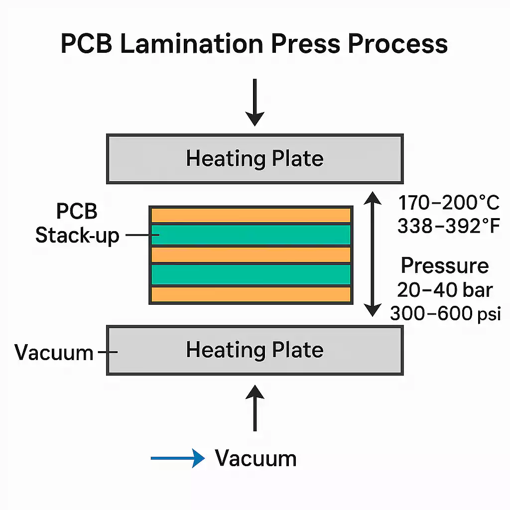
Modern presses often use multi-zone heating and programmable pressure ramps to optimize bonding and avoid defects like resin starvation or trapped air voids.
Step 4: Controlled Cooling
After the heat cycle, boards are gradually cooled under pressure to avoid:
- Thermal shock, which can cause cracks or delamination
- Warping, especially in high-layer-count or asymmetric stack-ups
Controlled cooling ensures dimensional stability and proper resin curing throughout the stack.
Step 5: De-Stacking and Post-Lamination Inspection
Once the lamination cycle is complete:
- Boards are removed from the press and separated from press plates and release films.
- A post-lamination inspection is performed to check for issues such as:
- Misregistration between layers
- Delamination or blistering
- Resin voids or uneven thickness
X-ray inspection may also be used in high-reliability applications to verify internal layer alignment and via quality.
Common Lamination Issues and Prevention Strategies
Even when using high-quality materials and equipment, PCB lamination can fail due to subtle process flaws or material mismatches. Understanding the most common lamination issues—and how to prevent them—is essential for ensuring product reliability and reducing costly rework or field failures.
Below are key lamination defects and practical strategies to mitigate them.
1. Delamination
What It Is:
Delamination refers to the separation of copper layers from the dielectric material, or the loss of adhesion between layers.
Common Causes:
- Excessive moisture in materials before lamination
- Incompatible or poorly cured prepreg
- Oxidized copper surfaces
- Incorrect lamination temperature or pressure profiles
Prevention:
- Pre-bake prepreg and core materials to remove moisture (typically at 105–125 °C for 4–6 hours)
- Use fresh, properly stored prepregs with controlled resin content
- Apply oxide or oxide-alternative treatments to enhance adhesion
- Optimize lamination temperature ramp-up and dwell times
2. Resin Voids and Starvation
What It Is:
Voids are air pockets or resin-deficient areas between layers, which weaken structural integrity and may cause electrical failure.
Common Causes:
- Inadequate resin flow from prepreg
- Insufficient pressure during lamination
- Contaminants or uneven lay-up
Prevention:
- Use the correct prepreg type and quantity based on the stack-up and copper fill
- Ensure even pressure distribution in the lamination press
- Maintain clean, debris-free surfaces during lay-up
- Consider vacuum-assisted lamination for high-layer-count boards
3. Layer Misregistration
What It Is:
Misalignment between internal layers can cause drill and routing issues, leading to open vias or faulty connections.
Common Causes:
- Inaccurate mechanical alignment during lay-up
- Core and prepreg dimensional instability (due to moisture or heat)
- Poor registration pin or tooling hole precision
Prevention:
- Use optical alignment systems or precision tooling pins
- Pre-bake cores to reduce expansion
- Control room temperature and humidity in the lay-up area
- Use symmetrical stack-ups to minimize warpage
4. Blistering or Bubbles
What It Is:
Gas or moisture trapped between layers during lamination can expand under heat, forming visible blisters or internal bubbles.
Common Causes:
- Incomplete degassing or moisture removal
- Low vacuum pressure during lamination
- Fast heating rate that traps volatiles
Prevention:
- Always bake prepregs and cores before lamination
- Use a vacuum lamination press if available
- Gradually ramp up temperature to allow gas escape before resin gels
5. Warping and Bow/Twist
What It Is:
Distortion in the final PCB shape, which can cause assembly and fitment issues in enclosures.
Common Causes:
- Asymmetrical layer stack-up
- Uneven copper distribution across layers
- Mismatched material properties (CTE, resin flow)
Prevention:
- Design balanced stack-ups with mirrored copper layouts
- Ensure even copper coverage on each layer (use copper pour if needed)
- Match prepreg and core materials for consistent expansion rates
Process Optimization and Practical Tips for Reliable PCB Lamination
While understanding the standard PCB lamination process is essential, true manufacturing excellence comes from optimizing each step for your specific application. Whether you're producing high-layer-count server boards or compact RF modules, fine-tuning your lamination process can improve yield, reduce defects, and enhance long-term performance.
Here are key optimization strategies and industry best practices to achieve consistent, high-quality lamination results:
1. Optimize Lamination Profiles (Temperature, Pressure, Time)
- Controlled Heating Ramp-Up: Avoid overheating the resin too quickly. A ramp rate of 2–4 °C/min is ideal to prevent resin voids and promote even flow.
- Appropriate Dwell Time: Maintain target temperature and pressure long enough (typically 60–120 minutes) to allow full resin cure and void elimination.
- Multi-Zone Press Control: Use presses with programmable heating zones and staged pressure application for complex or thick stack-ups.
2. Use Pre-Baking to Reduce Moisture Risks
Moisture is a major cause of delamination and blistering. Bake materials before lamination to remove residual moisture:
| Material | Typical Bake Condition |
|---|---|
| Prepreg sheets | 105–125 °C for 4–6 hours |
| Core laminates | 125 °C for 6–8 hours |
| Finished inner layers | 125 °C for 2 hours (post-etch) |
Store baked materials in a dry cabinet or vacuum-sealed bags if not used immediately.
Design Balanced Stack-Ups
- Use symmetrical copper layer designs to prevent warpage and bow/twist.
- Balance dielectric thickness and copper weights across the centerline.
- Avoid large copper density differences between adjacent layers.
A well-balanced stack-up not only improves lamination quality but also helps with impedance control and mechanical stability.
4. Match Material Properties Across Layers
- Align CTE (Coefficient of Thermal Expansion) and Tg (Glass Transition Temperature) values between core and prepreg materials.
- For high-speed or RF boards, match dielectric constant (Dk) and loss tangent (Df) across all insulating layers to minimize signal distortion.
Inconsistent material properties can lead to differential expansion, delamination, or impedance variation.
5. Use Vacuum Lamination or Vacuum Assist Systems
Vacuum-assisted lamination systems improve:
- Resin flow into tight spaces or dense via structures
- Void elimination between layers
- Laminate surface flatness
These systems are especially helpful for HDI, RF, and rigid-flex PCBs.
6. Inspect Frequently with Non-Destructive Testing (NDT)
- Use X-ray inspection to verify internal layer alignment and identify voids.
- Apply ultrasound scanning or C-scan imaging to detect delamination in high-reliability boards (e.g., aerospace or defense applications).
- Perform cross-section analysis during pilot runs to validate lamination quality.
Routine process audits help maintain consistency across production batches.
7. Document and Standardize Process Parameters
- Maintain detailed lamination process recipes by stack-up type and board thickness.
- Use Statistical Process Control (SPC) charts to monitor temperature, pressure, and dwell time trends.
- Keep logs of material batch numbers, bake times, and press settings to trace back issues if failures occur.
A data-driven approach enables faster troubleshooting and continuous improvement.
Conclusion
PCB lamination is a critical process that ensures the structural integrity and electrical performance of multilayer circuit boards. Whether for standard or high-density designs, proper bonding between copper and dielectric layers is essential to avoid failures such as delamination, warping, and resin voids.
By selecting compatible materials, maintaining moisture control, and using optimized lamination profiles, manufacturers can achieve consistent, high-quality results. Techniques like balanced stack-up design, pre-baking, and vacuum-assisted lamination further reduce the risk of defects.
As PCB technology advances, mastering the lamination process is key to delivering reliable, high-performance boards across industries.