

Introduction
Printed Circuit Boards (PCBs) are the foundational building blocks of modern electronics. Found in everything from smartphones and laptops to medical devices and automotive systems, PCBs not only provide mechanical support but also electrically connect components, allowing them to function cohesively. However, not all PCBs are created equal.
Understanding the various types of PCBs—such as single-sided, double-sided, multilayer, rigid, flexible, metal-core, ceramic, and high-density interconnect (HDI)—is crucial. Each type is specifically designed with unique features, strengths, and limitations, making it more suitable for certain applications over others. Choosing the right PCB type directly impacts performance, reliability, production costs, and even product lifespan.
In this comprehensive guide, we'll explore the main categories of PCBs, explain their structural differences, outline their advantages and disadvantages, and help you identify the ideal PCB type for your specific needs. Whether you're an engineer seeking advanced PCB solutions or a beginner learning the basics, this guide is tailored to provide clarity, detailed insights, and practical recommendations to support your decision-making process.
Types of PCBs
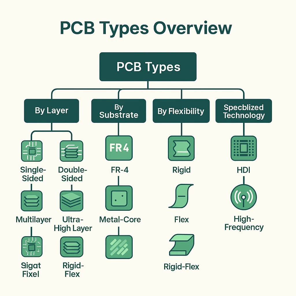
Printed Circuit Boards vary greatly in structure, materials, and complexity. Understanding their classifications is essential for making informed decisions in product development and manufacturing.
Below is a broad overview of PCB types, organized by key differentiators:
By Number of Layers
1. Single-Sided PCBs
Featuring conductive material on only one side, single-sided PCBs are the simplest and most economical. They're widely used in basic electronics due to their simplicity, affordability, and ease of mass production.
2. Double-Sided PCBs
With conductive layers on both sides, double-sided PCBs accommodate higher circuit density and more complex circuits compared to single-sided PCBs, making them suitable for moderately complex electronic products.
3. Multilayer PCBs
Consisting of three or more layers of conductive material separated by insulating layers, multilayer PCBs allow for greater complexity, improved signal integrity, and compact size. They're commonly found in smartphones, computers, and advanced electronics.
4. Ultra-High-Layer PCBs
Typically exceeding eight layers and potentially reaching dozens, these PCBs serve high-performance, mission-critical electronics where space is limited, such as servers, telecommunications equipment, and aerospace applications.
By Material/Substrate
1. FR-4 (Glass-Reinforced Epoxy Laminate)
The most common PCB substrate material, FR-4 offers strength, stability, and affordability. It's widely used for general-purpose electronics.
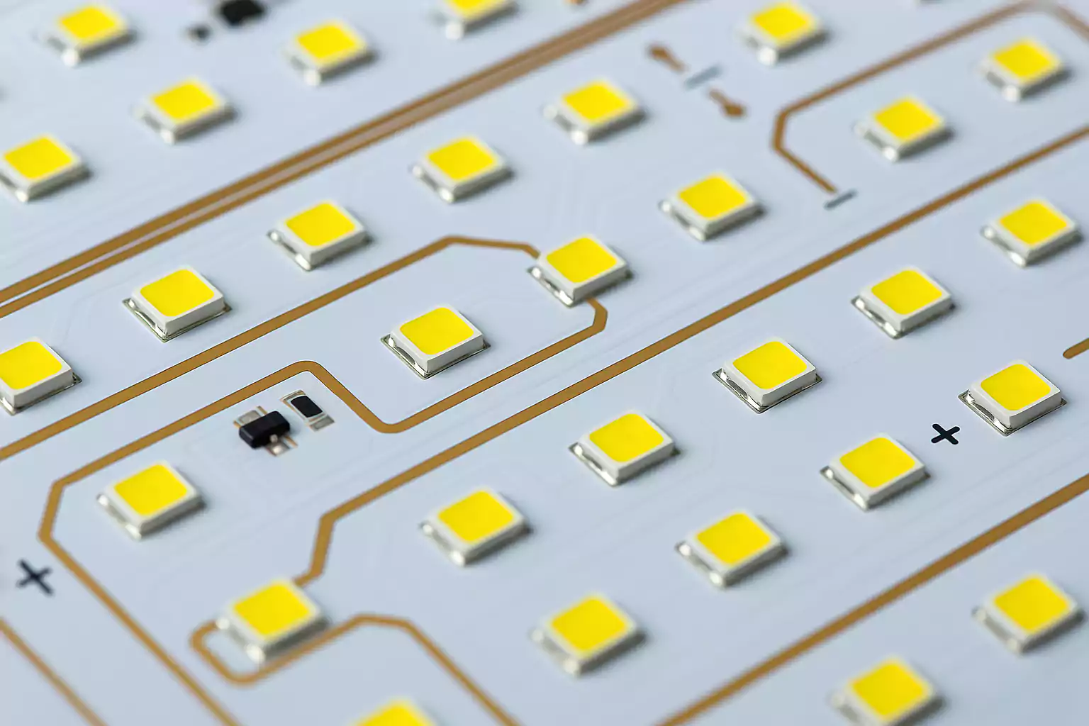
2. Metal-Core (Aluminum, Copper)
Metal-core PCBs provide superior thermal conductivity and heat dissipation, making them ideal for high-power applications like LED lighting and power electronics.
3. Ceramic PCBs
Known for exceptional thermal conductivity, durability, and insulation properties, ceramic PCBs are commonly used in high-frequency and high-temperature applications, including automotive, aerospace, and high-power electronics.
By Flexibility
1. Rigid PCBs
The traditional PCB type, constructed from solid substrate material, providing rigidity and strength. They are standard in consumer electronics, computers, and appliances.
2. Flexible PCBs (Flex PCBs)
Built from flexible substrates (often polyimide), flex PCBs enable dynamic bending, folding, or twisting. They are essential in wearables, medical devices, automotive wiring, and other space-constrained applications.
3. Rigid-Flex PCBs
Combining rigid and flexible elements, rigid-flex PCBs offer the structural benefits of rigid boards and the versatility of flexible boards, commonly used in aerospace, medical implants, and compact electronic systems.
By Specialized Technology
1. High-Density Interconnect (HDI) PCBs
Designed for miniaturization and complex routing, HDI PCBs utilize advanced via technologies (microvias, buried vias, blind vias), enabling smaller footprints, higher component density, and improved signal integrity. They're commonly found in advanced smartphones, tablets, and wearable devices.
2. High-Frequency PCBs
Optimized for RF and microwave frequencies, these PCBs use special substrates with stable dielectric properties. They're ideal for telecommunications, radar systems, and satellite communications.
PCB Types in Detail
Let's explore each PCB type individually to better understand their characteristics, advantages, limitations, and common uses.
| PCB Type | Structure | Advantages | Disadvantages | Typical Applications |
|---|---|---|---|---|
| Single-Sided | One conductive layer on one side | Low cost, simple manufacturing | Limited complexity | Calculators, LED lighting, basic consumer electronics |
| Double-Sided | Two conductive layers connected by vias | Higher circuit density, moderate complexity | Higher cost and design complexity | Automotive dashboards, power supplies, consumer appliances |
| Multilayer | Multiple conductive layers separated by insulation | Compact, high complexity, improved performance | Higher cost, complex production | Smartphones, computers, GPS, medical electronics |
| Rigid PCB | Solid, inflexible substrates (usually FR-4) | Durable, cost-effective, stable | No flexibility, unsuitable for bending | Computers, TVs, printers, industrial equipment |
| Flexible PCB | Flexible substrate (polyimide) allowing bending | Space-saving, lightweight, reduces connectors | Higher cost, design complexity | Wearables, automotive wiring, medical devices, folding phones |
| Rigid-Flex PCB | Combination of rigid and flexible substrates | Combines durability with flexibility, reliable | High cost, complex production and design | Aerospace, medical imaging, cameras, foldable electronics |
| Metal-Core (MCPCB) | Metal substrate (aluminum/copper) for thermal management | Superior heat dissipation, durable, thermal stable | Higher cost, limited design flexibility | LED lighting, automotive headlights, solar panels |
| Ceramic PCB | Ceramic substrate for high thermal conductivity | Excellent heat dissipation, chemical resistance | High cost, brittle and susceptible to damage | RF circuits, automotive sensors, aerospace electronics |
| High-Density Interconnect (HDI) | Uses microvias, blind/buried vias, thin substrates | High-density, compact, improved signal performance | High cost, complex manufacturing | Smartphones, high-performance computing, medical implants |
| High-Frequency PCB | Specialized substrates for RF/microwave frequencies | Stable dielectric properties, low signal loss | Higher cost, complex design | Telecom (5G), radar, wireless IoT, satellite systems |
Understanding these PCB types, their structures, strengths, limitations, and typical applications enables you to make informed choices tailored precisely to your specific project requirements.
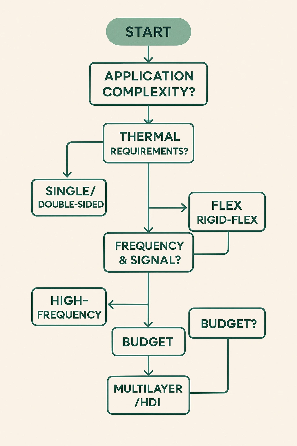
PCB Comparison Matrix and Selection Process
Selecting the right PCB type is critical for product performance, cost efficiency, and long-term reliability. To simplify this decision-making, we've prepared a comparison matrix and a step-by-step selection process to help you identify the ideal PCB for your needs.
| Criteria | Single-sided | Double-sided | Multilayer | Rigid | Flex | Rigid-Flex | Metal-Core | Ceramic | HDI | High-Frequency |
|---|---|---|---|---|---|---|---|---|---|---|
| Cost | Low | Moderate | High | Low | High | Very High | High | Very High | High | High |
| Circuit Density | Low | Moderate | High | Moderate | Moderate | High | Moderate | Moderate | Very High | High |
| Thermal Performance | Low | Moderate | Good | Moderate | Moderate | Good | Excellent | Excellent | Good | Good |
| Flexibility | None | None | None | None | Excellent | Good | None | None | None | None |
| Mechanical Strength | Moderate | Good | Excellent | Excellent | Good | Excellent | Excellent | Excellent | Excellent | Good |
| Manufacturing Complexity | Low | Moderate | High | Moderate | High | Very High | Moderate | High | Very High | High |
| Miniaturization | Poor | Moderate | Good | Moderate | Good | Excellent | Moderate | Moderate | Excellent | Good |
| Reliability | Moderate | Good | Excellent | Good | Good | Excellent | Excellent | Excellent | Excellent | Excellent |
Step-by-Step PCB Selection Process
To guide your selection, follow this simple yet effective process:
Step 1: Determine the Application Requirements
- Identify the intended application (consumer electronics, automotive, aerospace, medical, etc.).
- Establish performance criteria such as size constraints, thermal demands, signal integrity, flexibility, and durability.
Step 2: Evaluate Circuit Complexity and Density
- For low complexity, choose single-sided or double-sided PCBs.
- Medium to high complexity typically demands multilayer or HDI PCBs.
Step 3: Assess Thermal Management Needs
- High-power or LED-based applications benefit greatly from metal-core or ceramic PCBs.
- Standard electronics can typically use rigid FR-4 PCBs or standard multilayers.
Step 4: Identify Space and Flexibility Constraints
- For highly compact designs, consider HDI or multilayer PCBs.
- Applications needing flexibility or dynamic bending require flex or rigid-flex PCBs.
Step 5: Consider Frequency and Signal Requirements
- High-frequency or RF applications (e.g., telecom, radar) require specialized high-frequency PCBs.
- High-speed digital circuits benefit from HDI or multilayer PCBs due to improved signal integrity.
Step 6: Review Budget and Cost Efficiency
- Cost-sensitive projects often choose single or double-sided rigid PCBs.
- If performance outweighs cost, options include rigid-flex, HDI, or ceramic PCBs.
Key Considerations for Optimal PCB Selection
- Always balance cost against critical performance needs.
- Prioritize reliability and long-term performance in demanding environments.
- Consult manufacturers early in the design phase to ensure manufacturability and avoid costly redesigns.
Manufacturing & Material Considerations
When designing or selecting a PCB, careful attention to manufacturing processes and material selection is essential. Proper choices significantly impact PCB quality, cost, reliability, and overall performance.
Substrate Materials
The substrate material serves as the foundation for the PCB, influencing mechanical strength, thermal properties, electrical performance, and cost. Common PCB substrates include:
1. FR-4 (Glass Epoxy Laminate)
- Pros: Cost-effective, widely available, durable.
- Cons: Limited thermal conductivity, moderate dielectric constant.
- Applications: General-purpose electronics, consumer devices, computing equipment.
2. Metal-Core Substrate (Aluminum, Copper)
- Pros: Excellent thermal conductivity, durability, mechanical stability.
- Cons: Higher cost, heavier, less flexibility in design.
- Applications: High-power electronics, LED lighting, power converters.
3. Ceramic Substrate (Aluminum Oxide, Aluminum Nitride)
- Pros: Exceptional heat dissipation, high mechanical strength, stable dielectric properties.
- Cons: High cost, brittleness, complex manufacturing.
- Applications: RF circuits, automotive sensors, aerospace electronics, power modules.
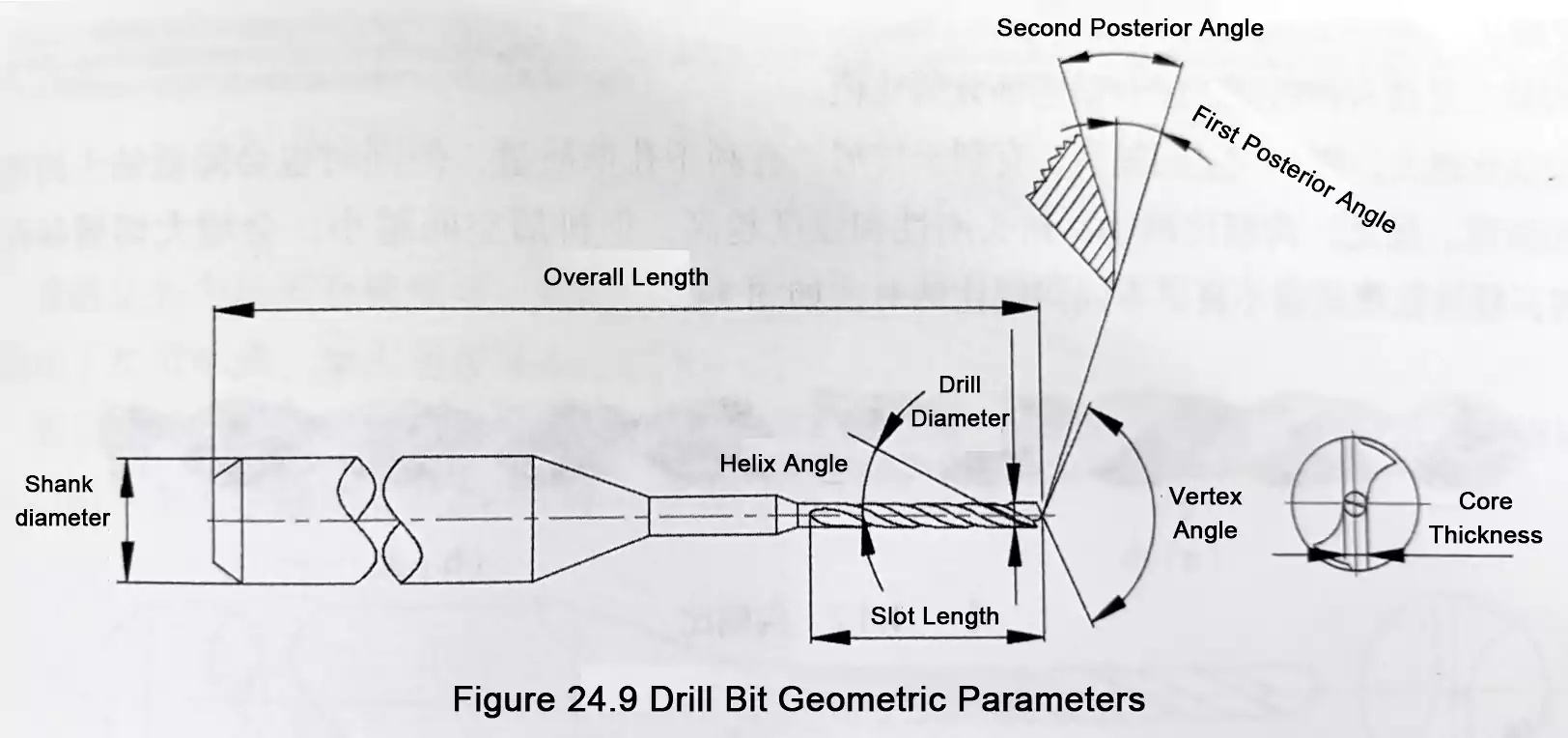
Via Types and Considerations
Vias (vertical interconnect accesses) provide electrical connections between layers. Selecting the appropriate via type impacts performance, space utilization, and costs.
1. Through-Hole Vias:
Connect all PCB layers.
Suitable for simpler designs; cost-effective and reliable.
2. Blind Vias:
Connect outer layers to inner layers, but do not pass completely through the board.
Allow higher circuit density and miniaturization.
3. Buried Vias:
Only connect internal layers, invisible from outside layers.
Ideal for dense, multilayer, or HDI PCBs; increases manufacturing complexity.
4. Microvias:
Small vias (≤0.15 mm) suitable for HDI PCBs.
Excellent for dense, high-speed designs; more expensive but improves signal integrity significantly.
PCB Stack-Up Design
The arrangement and thickness of PCB layers (stack-up) impact signal integrity, thermal dissipation, EMI performance, and mechanical robustness.
Key considerations include:
1. Number of Layers: Higher layers increase complexity and cost but enhance circuit density and EMI control.
2. Dielectric Thickness: Thinner dielectrics enable compact designs and improve high-frequency performance but may increase cost and manufacturing difficulty.
3. Impedance Control: Accurate impedance control is crucial for high-frequency signals, ensuring minimal signal reflection and stable transmission.
Thermal Management
Effective thermal management ensures component longevity, reliability, and optimal operation:
1. Heat Dissipation Methods:
- Metal-core substrates
- Thermal vias
- Heat sinks or heat spreaders
- Copper thickness adjustments (heavier copper layers)
2. Material Thermal Conductivity
Choose materials (e.g., aluminum substrates, ceramic) offering superior heat conduction in high-power applications.
Assembly & Manufacturing Complexity
PCB design choices directly affect manufacturing complexity and assembly efficiency:
1. Surface-Mount Technology (SMT) vs. Through-Hole:
- SMT allows miniaturization, automation, and improved performance but requires careful assembly processes.
- Through-hole offers reliability and simplicity but consumes more space.
2. Panelization & Board Shape:
- Proper panelization reduces manufacturing costs and optimizes the production process.
- Simple shapes minimize waste and production complexity.
Design for Manufacturability (DFM)
Early consideration of DFM ensures smoother production processes, reducing lead times and avoiding expensive redesigns:
- Maintain standard hole sizes, spacing, and trace widths.
- Clearly define and minimize via types to simplify production.
- Consult manufacturers early to align designs with production capabilities and cost optimization.
Solder Mask & Surface Finish
The selection of solder mask and surface finishes directly influences corrosion resistance, solderability, and durability:
1. Solder Mask
Protects copper traces from oxidation and shorts. Typically green, but other colors available for identification or aesthetics.
2. Surface Finish
HASL (Hot Air Solder Leveling): Cost-effective, good solderability, suitable for general electronics.
ENIG (Electroless Nickel Immersion Gold): Excellent corrosion resistance, flatness, suitable for high-reliability applications, more expensive.
OSP (Organic Solderability Preservative): Environmentally friendly, cost-effective, short shelf-life.
Emerging Trends & Technology Updates in PCBs
As electronics evolve rapidly, so do Printed Circuit Board (PCB) technologies. Keeping abreast of emerging trends is crucial for staying competitive and leveraging new opportunities. Here are some key advancements reshaping the future of PCB design and manufacturing:
1. Flexible and Stretchable Electronics
Flexible electronics, incorporating ultra-thin and stretchable PCBs, have unlocked innovative possibilities across industries. Built on advanced flexible substrates like polyimide or silicone, these PCBs adapt to dynamic shapes and movements.
Advantages:
- Exceptional flexibility and conformability
- Reduced weight and space
- Enhanced durability
Applications:
- Wearable health monitors and smart clothing
- Flexible displays and foldable smartphones
- Automotive and aerospace components
2. Printed Electronics and Inkjet PCB Manufacturing
Printing conductive inks directly onto substrates enables rapid prototyping, customization, and more sustainable production methods.
Advantages:
- Shorter development cycles and reduced production costs
- Environmentally friendly materials and processes
- Enables lightweight, thin, and flexible circuit designs
Applications:
- Smart packaging and RFID tags
- Disposable medical sensors
- Flexible antennas and IoT devices
3. Ball Grid Array (BGA) and Advanced Packaging
Advanced packaging solutions, like BGA, increase circuit density, performance, and reliability. BGA packages connect integrated circuits directly onto PCB surfaces, significantly reducing size and improving electrical performance.
Advantages:
- Reduced board space, increased component density
- Improved thermal and electrical performance
- Enhanced reliability for high-performance electronics
Applications:
- High-end processors and memory modules
- Smartphones, tablets, and compact electronics
- Automotive ECUs and aerospace avionics
4. 3D and Embedded Components
3D and embedded component technologies integrate passive and active components within the PCB layers, enhancing miniaturization and reducing assembly complexity.
Advantages:
- Significant size and weight reduction
- Enhanced electrical performance and reliability
- Reduced signal interference and improved thermal management
Applications:
- Compact medical devices (hearing aids, pacemakers)
- Military and aerospace electronics
- Portable consumer electronics and smartphones
5. High-Speed and High-Frequency PCB Materials
With the rise of 5G networks, IoT, and advanced computing, specialized PCB substrates designed for high-speed, high-frequency signals have become essential.
Advantages:
- Low signal loss and reduced electromagnetic interference (EMI)
- Stable electrical performance at high frequencies
- Improved reliability in demanding applications
Applications:
- 5G telecom infrastructure
- Automotive radar and ADAS systems
- Satellite communications and RF antennas
6. Sustainability and Eco-Friendly PCB Technologies
Environmental sustainability is increasingly influencing PCB manufacturing. Eco-friendly materials and processes are becoming standard in response to regulatory requirements and consumer expectations.
Key Trends:
- Lead-free soldering and halogen-free substrates
- Recyclable and biodegradable PCB materials
- Water-based manufacturing processes and sustainable waste management
Advantages:
- Reduced environmental impact
- Compliance with global regulations (e.g., RoHS, REACH)
- Enhanced corporate social responsibility and market reputation
7. Artificial Intelligence (AI) in PCB Design & Manufacturing
AI-driven software tools streamline PCB layout optimization, improve fault detection during production, and predict reliability issues, significantly accelerating design cycles and boosting manufacturing efficiency.
Benefits:
- Reduced design time and enhanced PCB performance
- Higher accuracy in fault detection and quality assurance
- Predictive maintenance and yield improvements in manufacturing
Applications:
- High-performance computing and servers
- Automotive electronics and robotics
- Precision manufacturing and aerospace systems
Industry Applications
PCBs are foundational components across various industries, each type uniquely optimized for specific application demands. Below we explore detailed examples, highlighting how different PCB types fulfill critical industry requirements:
| Industry | PCB Types Used | Typical Applications |
|---|---|---|
| Consumer Electronics | Multilayer, HDI, Flexible, Rigid-Flex | Smartphones, wearables, smart devices |
| Automotive | Metal-Core, Ceramic, Rigid-Flex | ECU, sensors, infotainment, electric vehicles |
| Medical and Healthcare | Flexible, Rigid-Flex, HDI, Ceramic | Implants, diagnostic imaging, portable devices |
| Aerospace & Defense | Rigid-Flex, Ceramic, HDI | Avionics, satellites, radar systems |
| LED Lighting | Metal-Core, Ceramic | Street lighting, residential/commercial LED lighting |
| Telecommunications (5G) | High-Frequency, HDI, Multilayer | Antennas, base stations, routers, switches |
| Industrial Electronics | Rigid, Multilayer, Metal-Core | Robotics, automation controls, power equipment |
FAQs
What is the main difference between HDI and standard multilayer PCBs?
HDI (High-Density Interconnect) PCBs use advanced fabrication techniques (such as microvias, blind and buried vias) to achieve higher component density, finer trace widths, and smaller board sizes compared to traditional multilayer PCBs. Standard multilayer PCBs typically have larger via sizes and lower circuit density.
When should I consider using metal-core PCBs instead of FR-4?
Consider metal-core PCBs for applications requiring superior thermal management, such as high-power LED lighting, automotive headlights, power electronics, and high-current devices. FR-4 PCBs are sufficient for general-purpose electronics where thermal dissipation is less critical.
Which PCB type offers the best balance between cost, complexity, and reliability?
Double-sided or standard multilayer PCBs generally offer the best balance. They accommodate moderate complexity, provide good reliability, and are cost-effective for most consumer and industrial electronics applications.
How do I decide if a flexible or rigid-flex PCB is necessary for my design?
Use flexible or rigid-flex PCBs when your product requires dynamic bending, compact installation, lightweight construction, or high reliability in space-constrained environments, such as wearable devices, medical implants, aerospace electronics, and automotive sensors.
What factors determine PCB manufacturing cost?
Key cost-determining factors include:
1. Number of layers
2. Type of substrate material (FR-4, metal-core, ceramic)
3. Via complexity (microvias, buried/blind vias)
4. Surface finishes (ENIG, HASL, OSP)
5. PCB thickness and size
6. Special fabrication processes (HDI, flexible substrates)
What is the environmental impact of different PCB types, and which is most eco-friendly?
Standard FR-4 PCBs using lead-free solder and halogen-free materials are generally the most eco-friendly due to easier recyclability. Metal-core and ceramic PCBs have higher environmental footprints due to specialized materials and more complex production methods. However, emerging printed PCB technologies using biodegradable substrates and eco-friendly inks show great promise for sustainability.
How do high-frequency PCB materials differ from standard PCB materials?
High-frequency PCB materials have specialized dielectric substrates with lower dielectric constant (Dk) and lower loss tangent (Df), providing improved signal integrity and minimal signal loss at high frequencies. Standard PCB materials like FR-4 typically exhibit higher signal loss at frequencies above 1 GHz.
Are ceramic PCBs suitable for every high-temperature application?
Ceramic PCBs offer exceptional heat dissipation and thermal stability, making them suitable for high-temperature applications. However, their brittleness and higher cost may limit their practicality for some scenarios. Consider metal-core PCBs if mechanical flexibility or cost-effectiveness is a higher priority alongside good thermal management.
What is the advantage of using printed (inkjet) PCB technologies?
Inkjet PCB technology enables rapid prototyping, shorter production cycles, reduced waste, lower cost, and the possibility to print flexible or customized circuits on various substrates, including paper, polymers, or textiles. It's ideal for rapid development, flexible electronics, IoT applications, and low-cost disposable sensors.
Can I combine different PCB types in a single project?
Yes, combining PCB types within a single product is common and advantageous. For instance, you might use a metal-core PCB for a high-power LED module, a flexible PCB for connections requiring movement, and an HDI or multilayer rigid PCB for processing and control components. Combining PCB types optimizes performance, cost, and functionality tailored precisely to application needs.
Final Thoughts
Selecting the ideal PCB type is more than a technical choice—it’s a strategic decision impacting product success, profitability, and brand reputation. By carefully considering application needs, engaging closely with manufacturing experts, and proactively leveraging emerging PCB technologies, you will position your projects to excel in performance, reliability, and market competitiveness.
Use this guide as your roadmap to informed, effective PCB decision-making—ensuring your electronic products achieve their fullest potential.