


Printed circuit boards come in many types, but when it comes to carrying high current or managing heat, thick copper PCB—also known as heavy copper PCB—stand out. These boards utilize an increased copper thickness within the layers and traces to enhance conductivity, mechanical strength, and heat dissipation.
In this guide, you’ll learn what thick copper PCBs are, how they are made, and why they are essential for power electronics, automotive, and industrial systems.
What Is a Thick or Heavy Copper PCB?
A standard PCB usually uses 1 oz copper, which means one ounce of copper is spread evenly over one square foot of board area.
- 1 oz copper = about 35 µm (micrometers) = 1.37 mil of copper thickness.
When the copper weight increases to 3 oz (105 µm) or more per layer, it is typically referred to as a heavy copper PCB. Boards with 8 oz to 20 oz copper are often referred to as extra-heavy copper PCBs.
Compared to standard PCBs, thick copper boards have wider and thicker copper traces, allowing more current to pass through with lower resistance. The extra copper also improves thermal conductivity and mechanical durability, making them ideal for harsh environments and power-intensive designs.
When to Choose Thick Copper
You don’t need a heavy copper board for every design. It’s best used when your circuit must:
- Carry high current — such as power converters, amplifiers, and power distribution systems.
- Handle strong thermal loads — for example, LED drivers, motor controllers, or inverters that continuously generate heat.
- Resist extreme conditions — including vibration, high temperature cycles, or mechanical stress in automotive, military, or industrial equipment.
Copper Weight, Thickness, and Current Capacity
Because “oz” is a weight measure, many engineers prefer to visualize copper in terms of thickness. Here’s a simple conversion table:
| 0.5 oz | 17 µm | 0.7 mil | Signal, control |
| 1 oz | 35 µm | 1.37 mil | Standard boards |
| 2 oz | 70 µm | 2.74 mil | Power circuits |
| 3 oz | 105 µm | 4.11 mil | Heavy copper PCB |
| 6 oz | 210 µm | 8.22 mil | Power distribution |
| 10 oz | 350 µm | 13.7 mil | Industrial, defense |
| 20 oz | 700 µm | 27.4 mil | Extreme applications |
In simple terms:
- Thicker copper = lower resistance = more current capacity.
The current-carrying capacity depends on the line width, copper thickness, and temperature rise. According to IPC-2152 guidelines, doubling the copper thickness can reduce temperature rise by 30–40% for the same current. That’s why designers use thick copper for power planes and high-current paths.
Design Rules for Heavy Copper PCBs
Designing with thick copper is not the same as with standard 1-oz boards. The following rules help ensure manufacturability and stable performance:
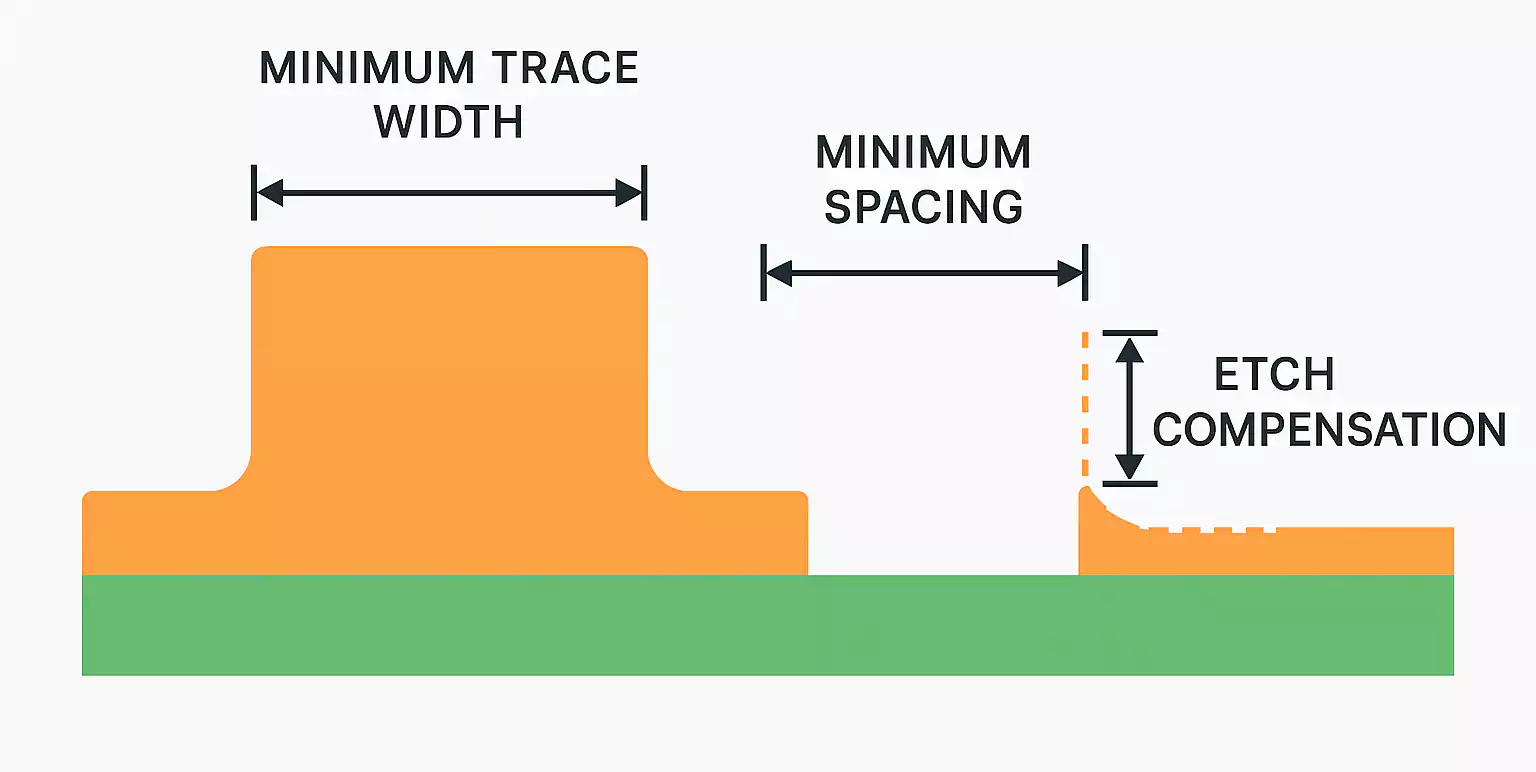
1.Trace Width and Spacing
As copper gets thicker, side etching becomes a bigger issue. The thicker the copper, the more difficult it is to maintain a tight line width and spacing.
Typical minimums:
- 3 oz copper: 8–10 mil minimum trace width/spacing.
- 6 oz copper: 12–15 mil.
- 10 oz and above: 20 mil or more.
2.Vias and Plating
Thick copper means thicker plating inside vias, which improves current-carrying capacity but can lead to uneven deposition. Use larger via diameters (≥ 0.3 mm finished) and through-hole copper thickness around 25–30 µm or more for high-current paths.
For heat management, place thermal vias under power components to conduct heat to other copper planes or to an external heatsink.
3.Solder Mask and Pads
Due to the higher topography, solder mask coverage may shrink or flow differently. Oversize pads slightly and adjust solder mask openings to prevent exposure misalignment.
4.Impedance and High-Speed Considerations
Thick copper changes the geometry of signal layers. The increased copper height lowers impedance, so the dielectric thickness may need to increase to maintain target values. For high-speed designs, communicate with the PCB supplier to fine-tune impedance control on thick copper layers.
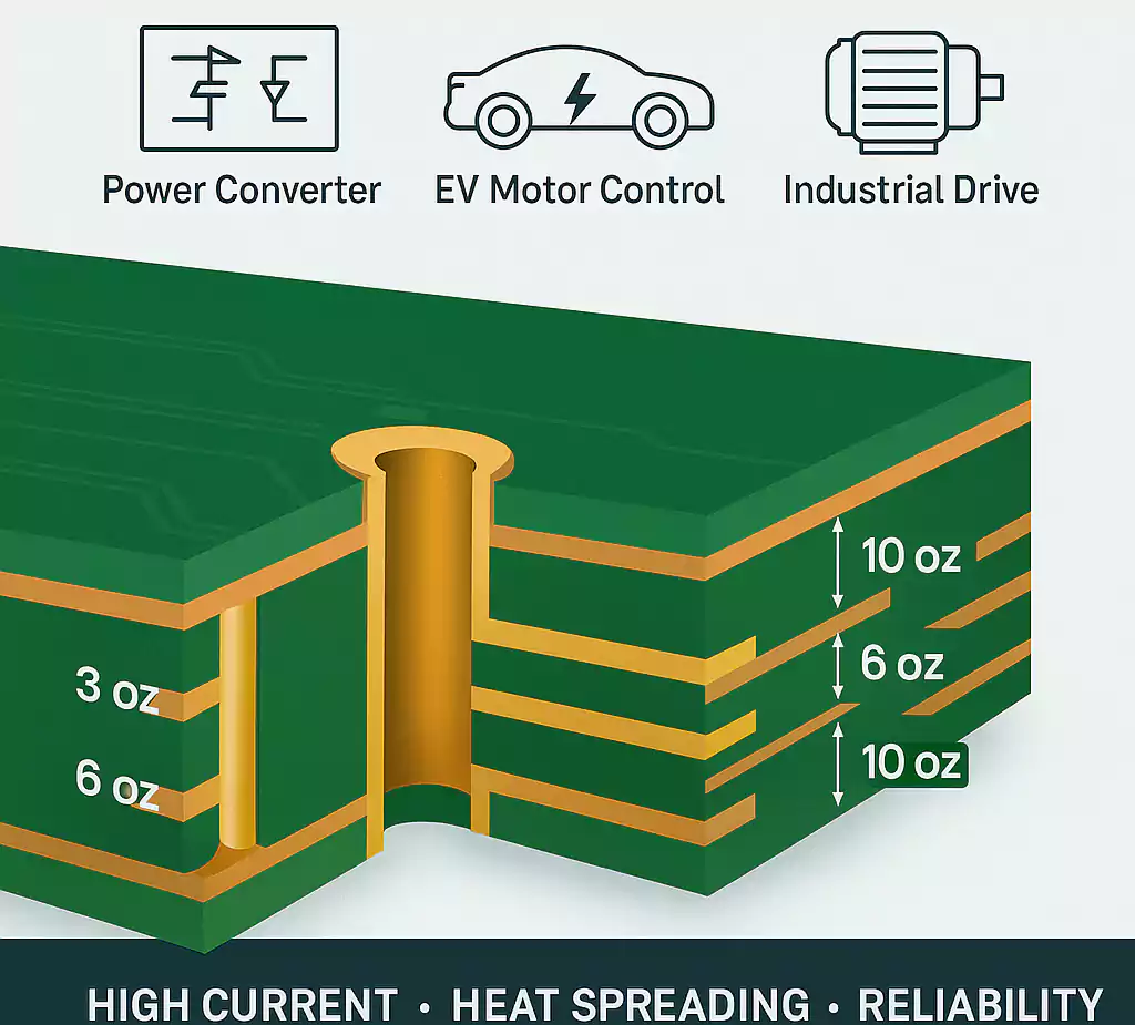
Typical Stackup Examples
To balance performance and cost, manufacturers often combine different copper weights on a single board.
Example 1 – 2-Layer 6 oz PCB
- Simple power bus or converter board.
- Each side features 6 oz of copper for handling currents of up to 50–100 A.
- Excellent thermal path, but thicker etching and heavier board.
Example 2 – 4-Layer PCB with 2 oz Outer / 3 oz Inner
- Balanced for power and signal integrity.
- Outer layers handle components and routing.
- Inner layers act as power planes with higher copper content for enhanced heat dissipation.
Example 3 – Mixed Heavy Layers (10–12 oz + Standard Layers)
- For high-power industrial or defense electronics.
- Top layers handle control signals (1–2 oz).
- The core or internal layer carries the heavy current (10–12 oz).
Thermal and Mechanical Reliability
One of the primary reasons for selecting thick copper is its thermal reliability. Thicker copper increases the board’s ability to spread and store heat.

In thermal tests, heavy copper traces significantly reduce the local temperature rise because heat spreads laterally through the copper plane. This reduces the need for large heat sinks or forced air cooling.
Mechanically, the stronger copper layer improves the PCB’s resistance to warping and cracking under thermal cycles. It also provides stronger pads that can withstand higher solder joint stress, such as that of large inductors or connectors.
Manufacturing Challenges and Cost Drivers
Producing thick copper PCBs is more complex than making standard boards. Several key factors affect both quality and cost:
1.Etching Control
When copper is 6 oz or thicker, chemical etching must remove a lot of material. Uneven etching can create slanted sidewalls or undercuts. To manage this, manufacturers adjust etch time, chemistry, and compensation width in the artwork.
2.Plating Thickness and Uniformity
Thick copper needs a longer electroplating time. The challenge is keeping a uniform copper distribution across large panels. Uneven plating can cause thickness variation between fine traces and large planes.
3.Drilling and Alignment
Drilling through thick copper generates more heat and tool wear. Manufacturers use specialized drill bits and controlled feed rates to ensure clean holes and precise registration.
4.Cost and Lead Time
Due to the added process time—especially for plating and etching—thick copper PCBs are more expensive and may take longer to produce.
Typical cost factors:
- Copper weight per layer.
- Board thickness and layer count.
- Minimum line width and spacing.
- Required surface finish and testing steps.
5.Capability Window
A high-quality manufacturer like Fast Turn PCBs can usually produce:
- Up to 15 oz outer layer copper.
- Up to 12 oz inner layer copper.
- Minimum trace/space around 8–10 mil at 4 oz and larger spacing for higher weights.
- Board thickness from 0.6 mm to 6 mm.
- Common finishes: ENIG, ENEPIG, HASL-LF, OSP, Immersion Silver.
Real-World Applications
Thick copper PCBs are found in almost every field where power and heat are major challenges. Some typical examples include:
1.Power Electronics
Power converters, voltage regulators, and inverters utilize 3–10 oz copper planes to efficiently carry tens of amps, thereby reducing losses and heat buildup.
2.Automotive Systems
Electric vehicles, LED lighting, and motor controllers require high reliability in the face of vibration and temperature fluctuations. Heavy copper provides the robustness needed for long-term operation.
3.Industrial Equipment
Motor drives, power supplies, and sensors benefit from improved current distribution and thermal performance.
4.Renewable Energy and Defense
Solar inverters, energy storage systems, radar modules, and power amplifiers often use 10 oz or thicker copper to handle continuous heavy loads and harsh conditions.
Surface Finishes and Reliability
The surface finish protects copper from oxidation and ensures reliable soldering. For thick copper PCBs, selecting the right finish is crucial due to the large copper volume and potential uneven surfaces.
Common finishes include:
- ENIG (Electroless Nickel Immersion Gold) – smooth, flat, good for fine-pitch and long shelf life.
- ENEPIG – adds palladium for better wire bonding and corrosion resistance.
- HASL Lead-Free – affordable and robust, but less flat for dense SMDs.
- OSP – cost-effective, eco-friendly for short production runs.
- Immersion Silver – good conductivity and solderability for power circuits.
FAQs: Thick Copper PCB Basics
1. What is “1 oz copper thickness”?
1 oz copper means one ounce of copper spread over one square foot of board area. Its thickness is about 35 µm (1.37 mil).
2. What is the difference between Heavy and Extra Heavy Copper?
- Heavy Copper: 3–6 oz copper per layer.
- Extra Heavy Copper: 8–20 oz or more, used for extreme current and thermal management.
3. Can a Thick Copper PCB have impedance-controlled traces?
Yes, but the design must use thicker dielectrics and wider traces to achieve the target impedance. Tolerances become tighter, so early discussion with the PCB supplier is essential.
4. Can one board mix different copper weights?
Yes. Many stackups combine standard signal layers (1–2 oz) with heavy power layers (6–12 oz). However, mixed copper layers increase the complexity and cost of lamination.
5. What is the practical copper thickness limit?
Most reliable manufacturers can build up to 15 oz outer layers and 12 oz inner layers. Beyond that, process control and cost make production less practical.
Conclusion
Thick copper PCBs are a proven way to increase current capacity, thermal performance, and reliability in modern electronics. They allow compact power designs without sacrificing durability.
By understanding how copper weight, trace width, and stackup interact, you can design boards that perform better and last longer in demanding environments.

If you need heavy copper boards for your next high-power project, Fast Turn PCBs offers advanced manufacturing up to 15 oz copper, quick lead times, and consistent quality.