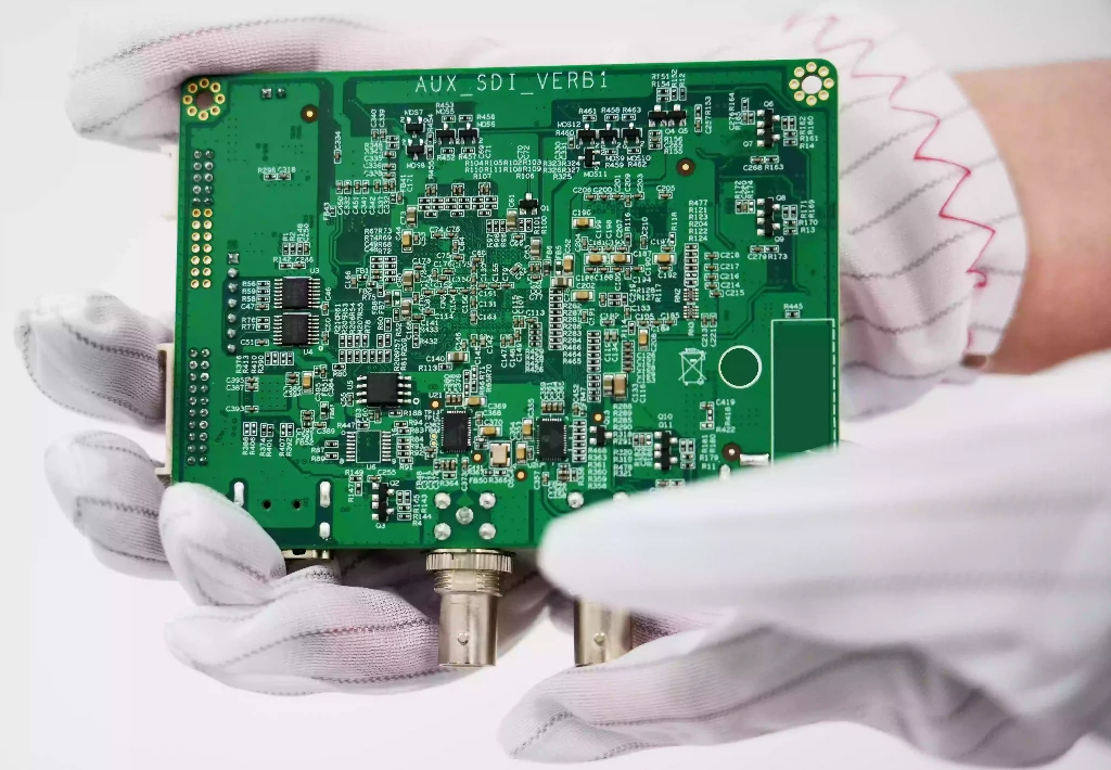
Introduction
Today’s electronic devices are pushing the limits of power and performance, especially in industries like automotive, industrial control, and renewable energy. Standard circuit boards with 1 oz copper thickness often can’t handle the high current or heat demands of these advanced applications. That’s where Thick Copper PCB—also called Heavy Copper PCB—come in.
Designed with much thicker copper layers than typical boards, thick copper PCBs offer better current-carrying capacity, improved thermal management, and greater mechanical strength.
In this article, we’ll break down what thick copper PCBs are, how they compare to standard 1 oz copper boards, and when you should consider using them.
What Is a Thick Copper PCB?
A Thick Copper PCB, also known as a Heavy Copper PCB, is a printed circuit board that features copper layers significantly thicker than the industry standard. While most standard PCBs use 1 oz copper thickness—equivalent to about 35 microns (µm) or 1.4 mils—thick copper PCBs typically use 2 oz, 3 oz, or even up to 10 oz of copper per square foot.
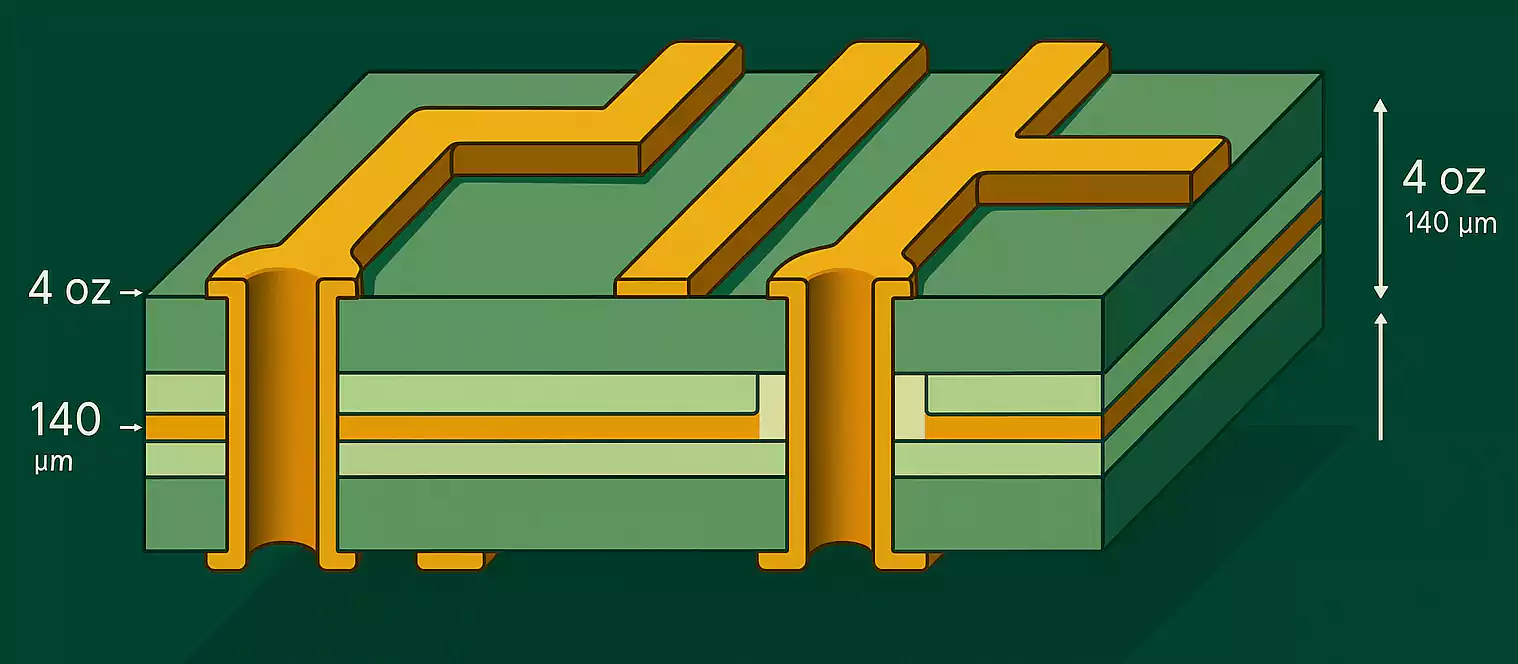
The term “oz” refers to the weight of copper spread over one square foot of area. As copper thickness increases, so does the board’s ability to carry higher current loads, dissipate heat more effectively, and withstand mechanical stress. That’s why thick copper boards are widely used in high-power and high-reliability applications.
In practical terms, thick copper PCBs are engineered to deliver performance where standard boards would fail—such as in power converters, battery management systems (BMS), motor controllers, and industrial power supplies.
1 oz Copper Thickness Explained
In PCB manufacturing, 1 oz copper thickness is considered the industry standard for most general-purpose circuit boards. But what does “1 oz” really mean?
The term refers to the weight of copper, 1 ounce spread evenly over one square foot of area. This equals a physical thickness of approximately 1.37 mils (0.00137 inches) or 35 microns (µm). It strikes a balance between cost, manufacturability, and electrical performance, which is why it's commonly used in signal layers, low-power designs, and consumer electronics.
However, 1 oz copper has current-carrying and thermal limits. It typically supports around 10–20 amps, depending on the trace width and whether the copper is on an internal or external layer. For high-power applications or designs that generate significant heat, 1 oz may not be sufficient.
That’s when designers consider moving to 2 oz, 3 oz, or heavier copper to improve current flow, reduce resistive losses, and enhance durability. Understanding the limitations of 1 oz copper is essential when choosing the right copper thickness for your PCB—especially in demanding environments like automotive, industrial control, and power supply systems
Why Choose Thick Copper PCBs?
Thick Copper PCB is the go-to solution when your design demands more than what standard 1 oz copper thickness can handle.
Here are the top reasons to choose a thick copper PCB:
1. Higher Current-Carrying Capacity
As copper thickness increases, so does the amount of current a trace can safely carry. Thick copper PCBs—ranging from 2 oz to 10 oz—are ideal for high-power applications like motor drivers, power converters, and battery management systems, where standard copper would overheat or fail.
2. Improved Thermal Management
Thicker copper layers help dissipate heat more efficiently, reducing the risk of hot spots and extending the life of components. This is especially important in designs where thermal performance directly impacts system reliability.
3. Enhanced Mechanical Strength
Heavy copper traces and plated vias add structural integrity, making the board more resistant to thermal cycling, vibration, and mechanical stress. This makes thick copper PCBs suitable for demanding environments like automotive, aerospace, and industrial equipment.
4. Space-Saving Design
Instead of using wider traces or external heat sinks, designers can use thicker copper to handle higher loads in a compact layout. This helps reduce board size and simplifies assembly.
5. Long-Term Reliability
Thick copper boards are built to last, especially in mission-critical systems where failure is not an option. Their robust construction ensures stable performance over time, even under extreme conditions.
Design Tips for Thick Copper PCB
Designing a Thick Copper PCB requires specific layout strategies to ensure reliability and manufacturability. Here are the most important tips to follow:
1. Use Proper Trace Widths
Higher copper thickness supports more current, but traces must also be wider to prevent overheating. Use IPC-2221 guidelines or calculators to size traces correctly based on current load and copper weight.
2. Increase Spacing Between Traces
Thicker copper needs wider spacing to avoid shorts and ensure clean etching. This is especially important for boards using 3 oz copper or more.
3. Design Robust Vias
Vias must be large enough and properly plated to handle higher current and thermal stress. For best results, consider via filling or via-in-pad when current demand is high.
4. Keep Copper Balanced Across Layers
Unbalanced copper can cause board warping. Maintain symmetrical layouts to ensure structural stability in multi-layer PCBs.
5. Account for Board Thickness
Thicker copper increases total board thickness. Make sure your mechanical design supports it, especially for connectors and enclosures
Manufacturing Considerations for Thick Copper PCBs
Designing Thick Copper PCB (2 oz, 3 oz, or more) requires thoughtful planning to ensure both electrical performance and manufacturability. Below are the core design considerations:
- Copper Thickness Selection
Choose the copper weight based on current-carrying requirements. For example, 2 oz copper can typically handle 20–30 amps on external layers with proper thermal management. - Trace Width and Spacing
Higher copper thickness requires wider traces and larger spacing to ensure reliable etching and to prevent thermal stress. Use IPC-2221 standards as a starting point. - Thermal Management
Include thermal vias, large copper areas, or heatsinks in the layout to dissipate heat effectively—especially in power-dense designs. - Mechanical Balance
Maintain copper weight symmetry across layers to prevent warping during lamination and ensure long-term structural integrity.
How to Select the Right Copper Thickness
| Copper Weight (oz/ft²) | Approx. Thickness | Current-Carrying Capacity (per IPC-2221, external layer) | Typical Applications |
|---|---|---|---|
| 1 oz | 35 µm (1.4 mils) | Up to 10–20 A | Consumer electronics, signal circuits, standard PCBs |
| 2 oz | 70 µm (2.8 mils) | Up to 25–35 A | Power supplies, motor drivers, industrial control |
| 3 oz | 105 µm (4.2 mils) | Up to 35–50 A | EV chargers, battery management systems (BMS), solar inverters |
| 4–6 oz | 140–210 µm | 50–80 A or more | High-power converters, aerospace, rail, heavy-duty automation |
| 8–10 oz+ | 280+ µm | 80 A+ | Military-grade systems, extreme environment electronics |
Conclusion
Thick Copper PCB provides clear advantages over standard copper boards—handling higher current, reducing heat buildup, and increasing reliability in demanding applications.
As electronics evolve toward higher power and tighter space constraints, these PCBs are becoming essential in power systems, automotive electronics, industrial equipment, and more.

Choosing the right copper weight—and working with a manufacturer experienced in thick copper PCB production—ensures your design performs reliably under real-world stress.
Need help selecting the right copper thickness? Contact Fast Turn PCB today for expert support and a fast, accurate quote.