Introduction
Whether you're a DIY electronics hobbyist assembling your first project or a manufacturing engineer overseeing large-scale production, one principle remains constant—every PCB must be tested. Printed Circuit Boards (PCBs) are the backbone of virtually all modern electronics, and even the slightest defect—like a solder bridge, broken trace, or misaligned component—can lead to product failure, costly recalls, or dangerous malfunctions.
Yet, PCB testing is often underestimated or poorly executed, especially in early-stage prototyping or small-batch production. Without a structured testing strategy, even the most well-designed circuits may not function as intended once powered on.
In this comprehensive guide, we'll walk you through everything you need to know about how to test a PCB—from basic visual inspection to advanced automated systems like in-circuit testing (ICT), flying probe, and AI-powered optical inspection.
Who Needs PCB Testing?
PCB testing isn't a one-size-fits-all process. Depending on your role, skill level, and the scale of your operation, your testing needs can vary dramatically. To deliver the most relevant strategies, let's look at four common user and how each benefits from effective PCB testing.
| User Type | Typical Use Case | Challenges | Testing Needs | Key Benefits |
|---|---|---|---|---|
| DIY Hobbyists | Small personal projects with Arduino, kits, or prototyping | Limited tools, lack of training, no access to professional equipment | Visual inspection, multimeter continuity tests, modular testing | Fewer build failures, saves time, avoids damaging components |
| Electronics Engineers | PCB design and prototyping for R&D or commercial products | Complex circuits, tight deadlines, design validation under pressure | Oscilloscope tracing, functional testing, simulation tools | Faster iteration, fewer redesigns, higher confidence before production |
| Production Test Engineers | High-volume testing in manufacturing environments | Speed vs. accuracy tradeoff, detecting small defects across large batches | ICT, flying probe testing, Automated Optical Inspection (AOI) | High throughput, consistent quality, reduced return/rework rates |
| Repair Technicians | Diagnosing and fixing faulty boards post-production | Lack of schematics, unknown fault symptoms, time constraints | Continuity testing, boundary scan, thermal imaging, signal tracing | Quicker diagnostics, lower replacement costs, better customer satisfaction |
Understanding your user profile helps determine the most appropriate PCB testing methods, tools, and workflows. Whether you're checking a single board on your workbench or overseeing thousands in production, this guide is tailored to help you test smarter and more effectively.
PCB Testing Workflow Overview
Before diving into tools and techniques, it's essential to understand the big picture—the overall workflow of testing a printed circuit board (PCB). Whether you're troubleshooting a prototype or validating a production unit, following a logical, step-by-step process will save you time, reduce errors, and ensure consistent results.
Below is an overview of the standard PCB testing workflow, which can be adapted depending on your goals, tools, and testing environment:
PCB Testing Process Flow
1. Visual Inspection
Check for obvious defects like solder bridges, missing components, poor alignment, or burned areas.
2. Continuity & Short Circuit Testing
Use a multimeter to verify that traces are connected as expected and no unintended shorts exist.
3. Power Supply Verification
Apply power gradually while monitoring current draw and checking voltage rails for correctness.
4. Component-Level & Functional Testing
Validate key components (e.g., ICs, sensors, regulators) and ensure basic functionality using signal tracing or functional test setups.
5. Automated Testing (If applicable)
Employ advanced techniques such as:
- In-Circuit Testing (ICT)
- Flying Probe Testing
- Automated Optical Inspection (AOI)
- Boundary Scan / JTAG
- ROSE Test for ionic contamination
6. Simulation & Signal Integrity Validation(Optional but recommended for complex boards)
Use EDA tools to simulate circuit behavior and assess timing, noise, and impedance issues.
7. Debugging & Retesting
Address any identified faults and re-run relevant tests to confirm fixes.
Why This Workflow Matters
- Minimizes risk of component damage by catching critical issues early (e.g., shorts before power-up).
- Supports modular debugging by isolating faults to specific stages or subsystems.
- Scales easily from manual testing for small projects to automated workflows in manufacturing.
This process creates a foundation for any PCB test strategy—regardless of the project size or complexity. In the next sections, we’ll dive deeper into each phase, exploring the tools, methods, and best practices that professionals use to ensure every board works exactly as designed.
Step-by-Step Breakdown of Each PCB Testing Phase
To ensure accurate, reliable results during PCB development and production, it's important to understand what each phase of the testing process involves. Here's a closer look at each step, with practical guidance, tools, and expert recommendations.
1. Visual Inspection
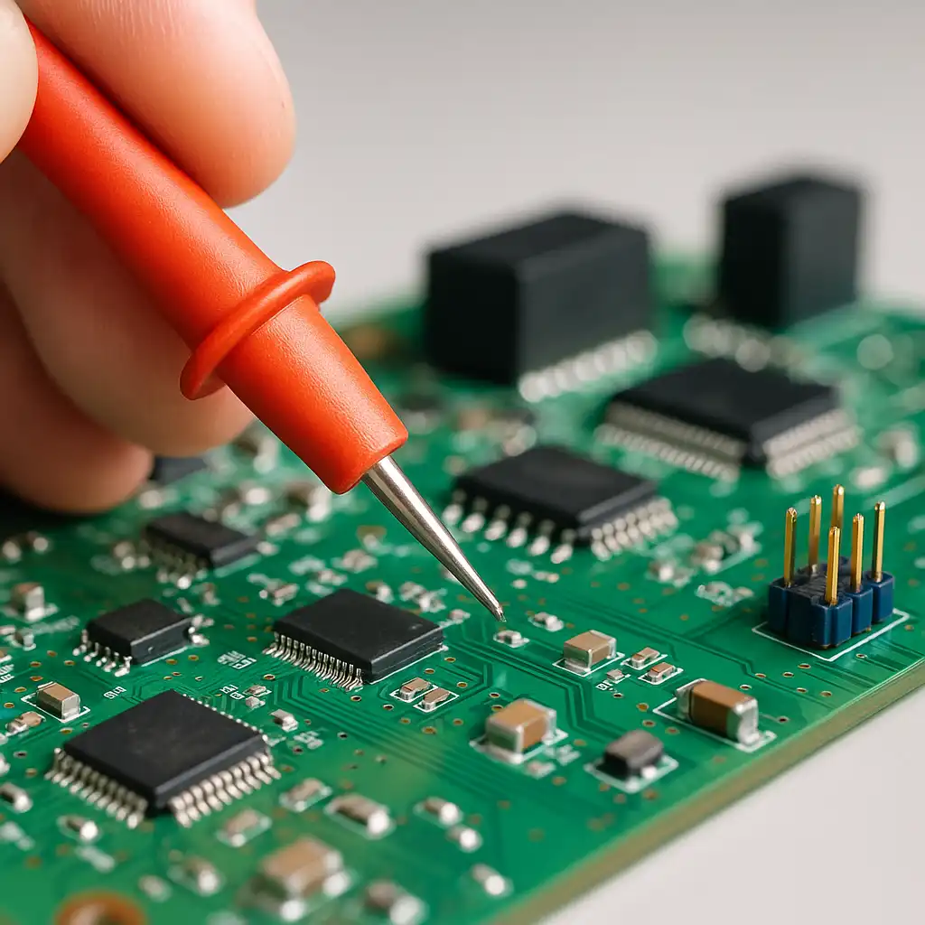
Purpose: Identify obvious manufacturing or assembly issues before applying power.
What to Look For:
- Solder bridges or cold joints
- Misaligned or missing components
- Burn marks, delamination, or damaged traces
- Silkscreen mismatches or polarity errors
Recommended Tools:
- Magnifying glass or microscope
- Ring light or inspection LED lamp
- Thermal camera (optional for power boards)
2. Continuity & Short Circuit Testing
Purpose: Ensure proper electrical connections and detect unintended shorts before powering the board.
How to Test:
- Use a digital multimeter in continuity mode
- Probe between pins, traces, and test points
- Pay attention to power and ground plane shorts
Common Checks:
- VCC–GND shorts
- Trace breaks or poor vias
- Signal path continuity (especially on multilayer boards)
3. Power Supply Verification
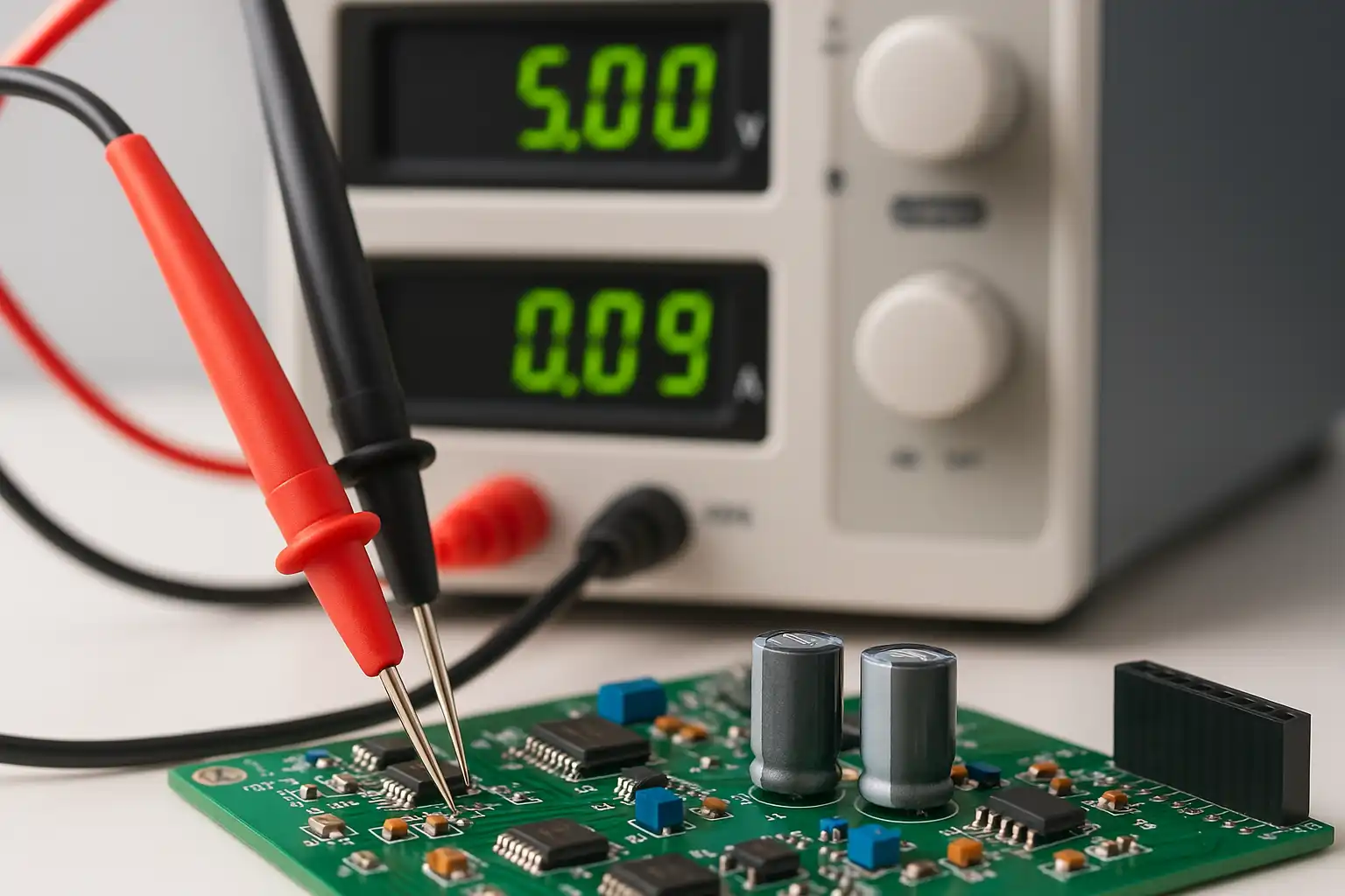
Purpose: Apply power safely and verify voltage rails without damaging components.
Procedure:
- Start with a current-limited bench power supply
- Measure voltage at each rail (e.g., 5V, 3.3V, Vcore)
- Check for abnormal heat or excessive current draw
Tools:
- Bench power supply with current limiting
- Multimeter and thermal camera
- Load simulator (for power modules)
4. Functional & Component-Level Testing
Purpose: Verify that individual components and basic subsystems behave as expected.
Steps:
- Test critical ICs using datasheets or functional scripts
- Validate oscillators, sensors, regulators, and MCUs
- Use an oscilloscope or logic analyzer to trace signals
Typical Use Cases:
- Confirm that clocks are oscillating
- Check I2C/SPI/UART communication
- Ensure sensor outputs respond to input conditions
5. Automated Testing (If Applicable)
Purpose: Increase speed, precision, and consistency during mass production or complex testing.
Common Methods:
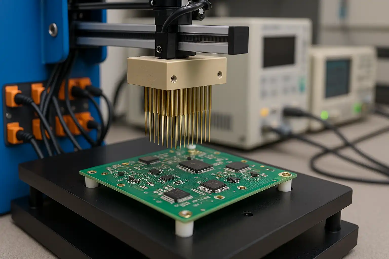
- In-Circuit Testing (ICT): Physical bed-of-nails probes to measure internal node values
- Flying Probe Testing: Electrically probes without a fixed fixture—ideal for prototypes
- Automated Optical Inspection (AOI): High-res camera system to detect soldering/placement errors
- Boundary Scan / JTAG: Digital chain testing for BGA and inaccessible nodes
- ROSE (Resistivity of Solvent Extract): Ionic contamination test for cleanliness
6. Simulation & Signal Integrity Validation
Purpose: Catch design flaws or performance bottlenecks using digital models before or after real-world tests.
Tools:
- SPICE-based simulation (e.g., PSpice, LTspice)
- Signal integrity tools (e.g., HyperLynx, OrCAD X)
- Crosstalk, impedance, and timing analysis
Use Cases:
- Validate high-speed traces (USB, HDMI, DDR)
- Simulate worst-case voltage drops or overcurrent conditions
- Identify clock skew or transmission line mismatches
7. Debugging & Retesting
Purpose: Fix and verify any issues identified in previous phases.
Common Debug Techniques:
- Divide and conquer: isolate sections of the board
- Compare against known-good units
- Swap suspected bad components
Documentation:
- Log all failed tests and results
- Maintain test revision history for product iterations
This detailed understanding of each stage enables more confident decisions and more successful products—whether you're testing one board or ten thousand.
Test Point Design & DFT (Design for Testability)
Testing efficiency begins at the design stage. Even the most advanced testing tools are ineffective if your PCB isn't designed to support them. That's where Design for Testability (DFT) comes in—a set of best practices that make your board easier, faster, and safer to test during development and production.
Why Test Point Design Matters
Test points are physical contact pads or pins placed on a PCB that allow easy electrical access to critical nets (such as power, ground, clock, or data lines). Well-placed test points can:
- Reduce troubleshooting time
- Improve accuracy and repeatability of tests
- Enable automated testing tools (ICT, flying probe)
- Lower long-term production and maintenance costs
Key Guidelines for Test Point Placement
To maximize the value of your test strategy, consider the following:
1. Cover Critical Nets
Include test points for:
- Power rails (e.g., 3.3V, 5V, VCORE)
- Ground
- Communication lines (I2C, SPI, UART, CAN)
- Clocks and resets
- Key outputs from sensors or microcontrollers
2. Maintain Proper Spacing
Follow IPC standards or manufacturer specs for spacing between test points to avoid shorts or mechanical probe conflicts. Typical minimum spacing: 50–100 mil (1.27–2.54 mm) depending on probe type.
3. Use SMD Pads or Through-Hole Vias
- SMD pads are compact and suitable for flying probe or manual testing.
- Via-in-pad or through-hole vias offer stronger mechanical contact, ideal for bed-of-nails ICT.
4. Label Clearly in the Silkscreen
Mark each test point with identifiers like TP1, TP2, or GND_TEST to assist technicians and reduce errors during manual or automated probing.
5. Group Related Test Points
Where possible, cluster test points logically:
- Power group (VCC, GND, EN)
- Communication group (TX, RX, SCL, SDA)
- Signal/debug group (CLK, RESET, INT)
This supports rapid testing via headers, custom test jigs, or ribbon cables.
DFT Beyond Test Points
Design for Testability goes beyond simply adding test pads. It includes:
Isolation for Subsystem Testing
Use 0Ω resistors or jumpers between power domains or blocks to isolate sections for independent testing.
Built-in Self-Test (BIST) Features
Embed microcontroller-driven test routines that toggle outputs or send known-good signals to help validate board functionality at boot.
Access to Programming & Debug Interfaces
Ensure your design exposes headers for:
- JTAG or SWD (for ARM-based MCUs)
- ISP (for AVR/ATmega)
- UART or USB for log output
Simulate Test Scenarios During Layout
Model how probes will physically access test points—especially in dense or double-sided boards—to avoid unreachable areas.
Common Pitfalls to Avoid
- ❌ Forgetting test points on ground or power rails
- ❌ Placing pads under components without access holes
- ❌ Using high-impedance nodes that give unreliable readings
- ❌ Relying solely on visual inspection without electrical access
Pro Tip: Think Like a Technician
Ask yourself:
- “Can someone test this board without the schematic?”
- “Can a flying probe or ICT machine reach all points?”
- “What happens if the firmware doesn't boot—can I still test power and clocks?”
Designing with these questions in mind builds a bridge between layout and testing, improving reliability and reducing time-to-market.
By applying DFT principles and carefully placing test points, you set the foundation for scalable testing—whether for one prototype or 10,000 production units.
Essential Testing Tools & Purchasing Guide
Whether you're testing a simple prototype or managing an entire production line, using the right tools is critical for accuracy, efficiency, and safety. The ideal setup depends on your budget, application, and the stage of testing (manual vs. automated).
Below is a breakdown of essential PCB testing tools, along with practical guidance on choosing the right equipment for your needs.
Must-Have PCB Testing Tools
| Tool | Purpose | Best For |
|---|---|---|
| Digital Multimeter (DMM) | Checks voltage, continuity, resistance, and current | All users – from hobbyists to pros |
| Oscilloscope | Visualizes voltage signals over time for waveform analysis | Engineers, advanced diagnostics |
| Logic Analyzer | Captures digital communication data (I2C, SPI, UART, etc.) | Embedded developers, protocol debugging |
| Bench Power Supply | Safely powers PCBs with adjustable voltage and current limits | Prototyping, safe power-on testing |
| Hot Air Station | SMD component rework and repair | Repair technicians, assembly testing |
| Function Generator | Injects known signals into circuits for response testing | Analog/mixed-signal testing |
| Thermal Camera or IR Thermometer | Detects overheating components, voltage drop issues | Power verification, debugging |
| Test Jig or Fixture | Holds PCB in place and routes connections for repeatable testing | Production-line testing |
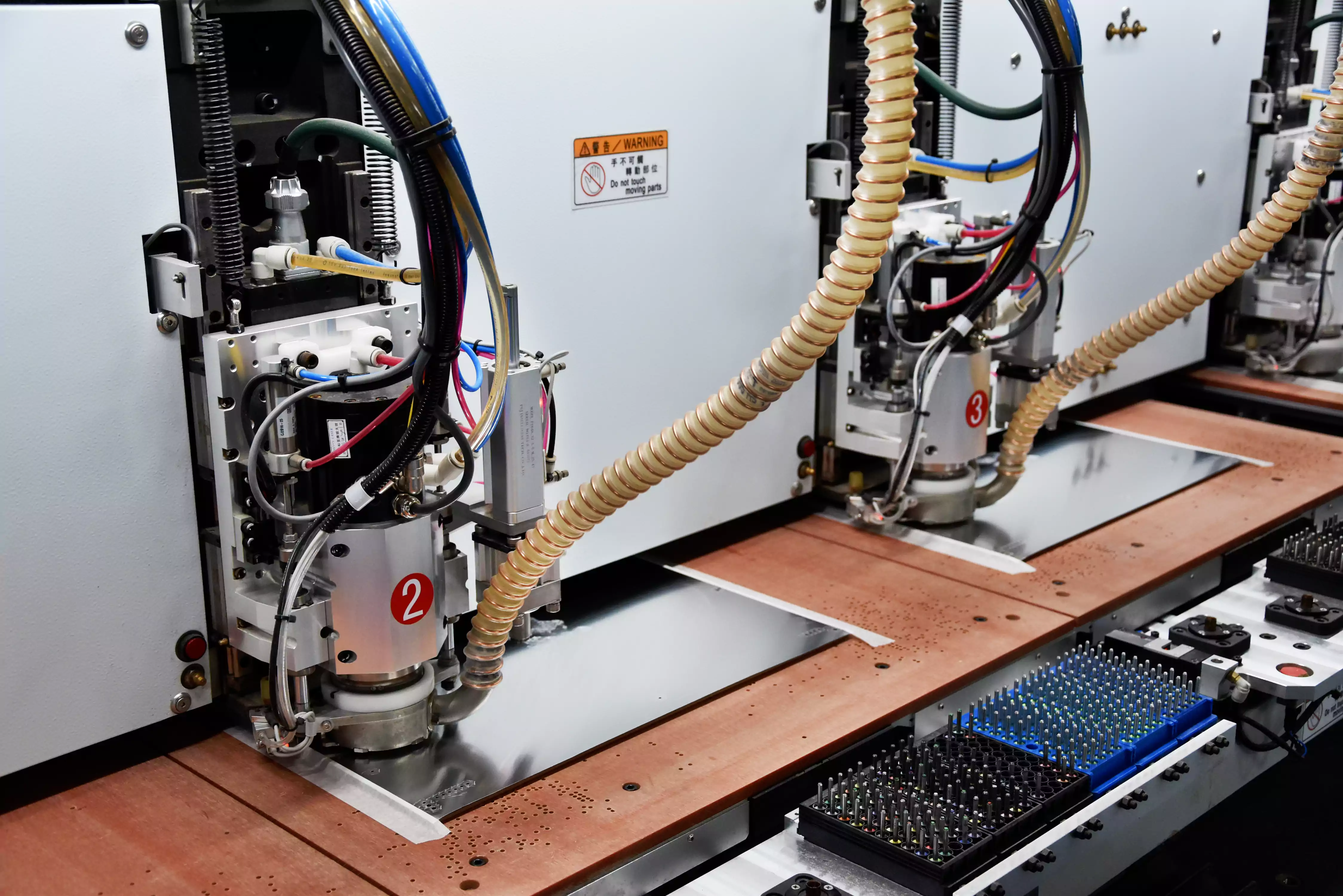
Automated Test Equipment (For Production & Complex Boards)
| Equipment | Function | Advantages | Considerations |
|---|---|---|---|
| In-Circuit Tester (ICT) | Probes each net to test continuity, resistance, capacitance, diode drops | Fast, repeatable, production-grade | Requires custom fixture; high upfront cost |
| Flying Probe Tester | Uses moving probes to test without fixture | Cost-effective for small runs or prototyping | Slower than ICT |
| Automated Optical Inspection (AOI) | Scans board with camera for visual defects | Non-contact, ideal for solder and alignment issues | Cannot test electrical functionality |
| Boundary Scan / JTAG | Tests digital devices and interconnects via serial interface | Great for BGA & inaccessible pins | Requires DFT and firmware integration |
| ROSE Tester | Measures ionic contamination on PCB surfaces | Ensures cleanliness, especially for aerospace/medical | Not needed for low-risk consumer products |
Tool Selection Tips
- Start Small if you're a beginner: a multimeter, oscilloscope, and adjustable power supply cover 80% of test needs.
- Go Modular: Instead of buying full test stations, build your bench gradually.
- Rent or Lease high-end tools like flying probe or ICT systems for short production runs.
- Buy Brands with Good Support: Fluke, Rigol, Keysight, Siglent, and Tektronix are known for reliability and long-term value.
- Use Open-Source Alternatives when budgets are tight – e.g., Saleae logic analyzer clones, DIY fixtures, or software simulators like LTspice.
Suggested Starter Kit (for prototyping & repair)
| Tool | Recommended Specs | Estimated Price (USD) |
|---|---|---|
| Digital Multimeter | Auto-ranging, continuity beep, true RMS | $30–$100 |
| Bench Power Supply | 0–30V, 0–5A, adjustable with current limiting | $60–$200 |
| Oscilloscope | 2-channel, 100 MHz or higher, USB or standalone | $200–$400 |
| Soldering + Hot Air Kit | ESD safe, digital temp control | $60–$150 |
| Logic Analyzer (USB) | 8-channel, 24MHz+, compatible with Sigrok/PulseView | $20–$80 |
With the right tools at your side, you'll be equipped to tackle any testing scenario—from rapid prototyping to automated high-volume inspection.
FAQs
My board doesn't power on—what should I check first?
Start by measuring the voltage across the main power rails (e.g., 3.3V, 5V, VCORE) using a multimeter. If voltage is absent or too low:
ㆍConfirm correct polarity from the power source
ㆍCheck for shorts between power and ground
ㆍUse a thermal camera to detect overheating components
ㆍTest the fuse (if any) and verify power switch operation
If there's a short, isolate sections of the board by desoldering jumpers or 0Ω resistors.
I hear a clicking sound or see flashing lights—what does that mean?
This usually indicates a power cycling loop, often caused by:
ㆍFaulty voltage regulator
ㆍOvercurrent protection triggering
ㆍWatchdog timer reset due to unstable power
Inspect capacitors and regulators, and verify current draw with a bench power supply.
My multimeter shows weird voltage readings. Is the component faulty?
Not necessarily. Some components, such as MOSFETs or ICs, have complex behavior that doesn't show up correctly on a simple DC voltage test. Try:
ㆍMeasuring under load with the circuit powered
ㆍUsing an oscilloscope to observe actual waveforms
ㆍVerifying with known-good replacement parts
How do I test a PCB with no firmware installed?
If your microcontroller or processor isn't programmed yet, focus on:
ㆍPower rail integrity and voltage levels
ㆍClock sources (e.g., crystal oscillators)
ㆍPassive components (resistors, capacitors)
ㆍSignal continuity and shorts
If possible, flash a minimal firmware that outputs test patterns via UART or toggles
What if I can't access a key signal with a probe?
Try one of the following:
ㆍUse test points designed during layout
ㆍProbe the pad of a passive component in-line with the signal
ㆍLeverage JTAG or boundary scan (if supported)
ㆍIf traces are internal (inner layers), consider simulation or built-in diagnostics
Do I need to retest after every fix or soldering step?
Yes—every change introduces a risk. Even small solder jobs can:
ㆍCreate solder bridges
ㆍDamage nearby traces with heat
ㆍLeave flux residue affecting high-frequency signals
Retesting ensures the board is still functioning as expected after each modificati
How many test points should a board have?
There's no fixed number, but a good rule of thumb is:
ㆍAt least one test point per power rail
ㆍKey communication lines and signal outputs
ㆍGround test points in accessible areas
ㆍDebug/test headers (UART, JTAG, etc.) for complex boards
Remember: More isn't always better—focus on accessibility and useful
Can I skip automated testing if I visually inspect everything?
No. Visual inspection can catch soldering or alignment issues, but electrical and functional faults often go undetected by eye. Automated testing methods like ICT or AOI dramatically improve detection rates and consistency.
Common Mistakes & Real-World Debugging Cases
Even experienced designers and technicians run into problems during PCB testing. Often, it's not the lack of tools but the overlooked basics or poor design assumptions that cause the most frustrating bugs.
This section highlights common mistakes in PCB testing and shares real-world debugging cases to help you identify, avoid, and resolve issues faster.
Common PCB Testing Mistakes
| Mistake | Impact | How to Avoid It |
|---|---|---|
| Powering up without a continuity check | Shorts can destroy ICs instantly | Always check resistance across power and ground before powering |
| No test points on key nets | Makes debugging nearly impossible later | Include test points for power, ground, clocks, and I/O lines |
| Relying only on visual inspection | Misses electrical faults and damaged components | Combine visual + electrical testing |
| Skipping retesting after rework | New issues may be introduced during soldering or adjustments | Re-test after every repair or board change |
| Using auto-ranging multimeters for timing | Can produce inaccurate or delayed readings | Use manual range or oscilloscopes for time-sensitive signals |
| Ignoring thermal signs | Overheating components go unnoticed until they fail | Use infrared thermometers or thermal cameras |
Case #1: Silent Board After Assembly
Symptom:
No lights, no heat, no response after applying power.
Root Cause:
A solder bridge between VCC and GND under the microcontroller caused an immediate short circuit.
Diagnosis Steps:
- Resistance check between power and ground = near 0 ohms
- No visible defect due to flux covering the bridge
- Removed MCU – short disappeared
- Re-soldered with clean pads – board powered up
Lesson Learned:
Always perform a pre-power continuity check—even on "perfect-looking" boards. Use flux cleaner and magnification to verify soldering.
Case #2: USB Not Recognized by Host
Symptom:
PCB powers up, microcontroller is running (blinking LED), but PC doesn't detect USB device.
Root Cause:
Improper pull-up resistor on the D+ line. USB interface didn't signal properly.
Diagnosis Steps:
- Logic analyzer showed no data on USB lines
- Verified schematic – pull-up was missing
- Soldered 1.5kΩ pull-up between D+ and 3.3V
- USB was recognized instantly
Lesson Learned:
Double-check interface specs and reference designs—especially for USB, I2C, and SPI. A single resistor can make or break communication.
Case #3: Intermittent Reset on Battery Power
Symptom:
Board works fine with USB power, but keeps resetting when powered by a LiPo battery.
Root Cause:
Inrush current from power-on caused voltage dip. The decoupling capacitor near the MCU was too far away physically on the PCB layout.
Diagnosis Steps:
- Oscilloscope showed 3.3V dropping to ~2.5V momentarily
- Added ceramic cap close to MCU VCC pin
- Problem resolved
Lesson Learned:
Don't underestimate layout effects. Good power distribution and capacitor placement are as important as the circuit itself.
Conclusion
Testing a PCB isn't just a technical task—it's a critical quality control step that bridges the gap between design and reliability. Whether you're building a DIY project, prototyping a new product, or preparing for large-scale manufacturing, following a structured and thoughtful testing process is essential to success.
In this guide, we've covered every stage of the PCB testing journey—from basic visual inspection and multimeter checks to advanced automated testing systems and design-for-testability strategies. Along the way, we've explored real-world challenges, shared practical tools, and highlighted the importance of thoughtful planning, clear test point design, and effective debugging techniques.