


Introduction: Why a Systematic Process Matters
When people search for “tecnograph process PCB,” they’re seeking a clear, end-to-end view of how a bare board becomes a reliable foundation for assembly. Getting this process right reduces prototype spins, stabilizes lead times, and prevents surprises at incoming inspection. This guide outlines a modern, production-grade PCB manufacturing flow—explaining each step, why it matters, and what data and tolerances are critical for first-pass success. It’s written for design engineers, sourcing managers, and startup teams who need practical clarity without unnecessary jargon.
Process Overview: From Data to Shipment
A robust tecnograph PCB process follows a consistent sequence:
CAM & DFM → Inner-layer imaging/etching → Lamination → Drilling (mechanical/laser) → PTH and copper plating → Outer-layer patterning/etching → Solder mask → Silkscreen/marking → Surface finish → Electrical test and inspection → Depanelization, cleaning, packaging.
Two factors tie this flow together:
• Clean, unambiguous build data
• Agreed-upon manufacturing targets for trace/space, via strategy, impedance, and surface finish
With these locked in, the remaining steps become predictable and measurable.
Front-End Engineering: CAM and DFM That Pass the First Time
Front-end engineering transforms your files into a buildable product.
- Data & Formats: Gerber X2, ODB++, or IPC-2581 are common. Include a clear stack-up, material details, drill chart, impedance goals with tolerances, and a test netlist. If assembly is required, add centroid data and a BOM for downstream checks.
- Panelization: Good panelization improves yield and throughput. Provide tooling rails with global fiducials and coupon areas, a depanelization strategy (V-scoring or routed tabs) aligned to component keep-outs, and test coupons if you need controlled impedance or coupon-based validation.
- Critical Tolerances: Align minimum trace/space with copper weight; set hole-to-copper clearances considering drill wander and registration; define differential impedance windows that match your material stack-up and outer-layer plating. If you’re pushing limits—HDI, fine-pitch BGA, or tight impedance—flag it so your fabricator can plan accordingly.
Materials and Stack-Up
Stack-up is the board’s DNA. It governs impedance, loss, flatness, and thermal performance.
- Core Choices: For general digital designs, FR-4 variants with suitable Tg and thermal expansion are effective. High-speed/RF designs may require low-Dk/low-Df laminates for controlled loss and skew. Always document Dk/Df values at your operating frequency, not just at 1 MHz.
- Copper Weight: Outer layers often start thinner and build copper during plating; inner layers use rolled or electro-deposited foils. Heavier copper allows higher current and thermal capacity but widens etched features and affects registration. Ensure your minimum trace/space is realistic for the copper weight and etch chemistry.
- Symmetry and Warpage: Keep layer pairs symmetrical to reduce bow and twist, and coordinate prepreg resin flow for proper fill around heavy copper areas and buried structures.
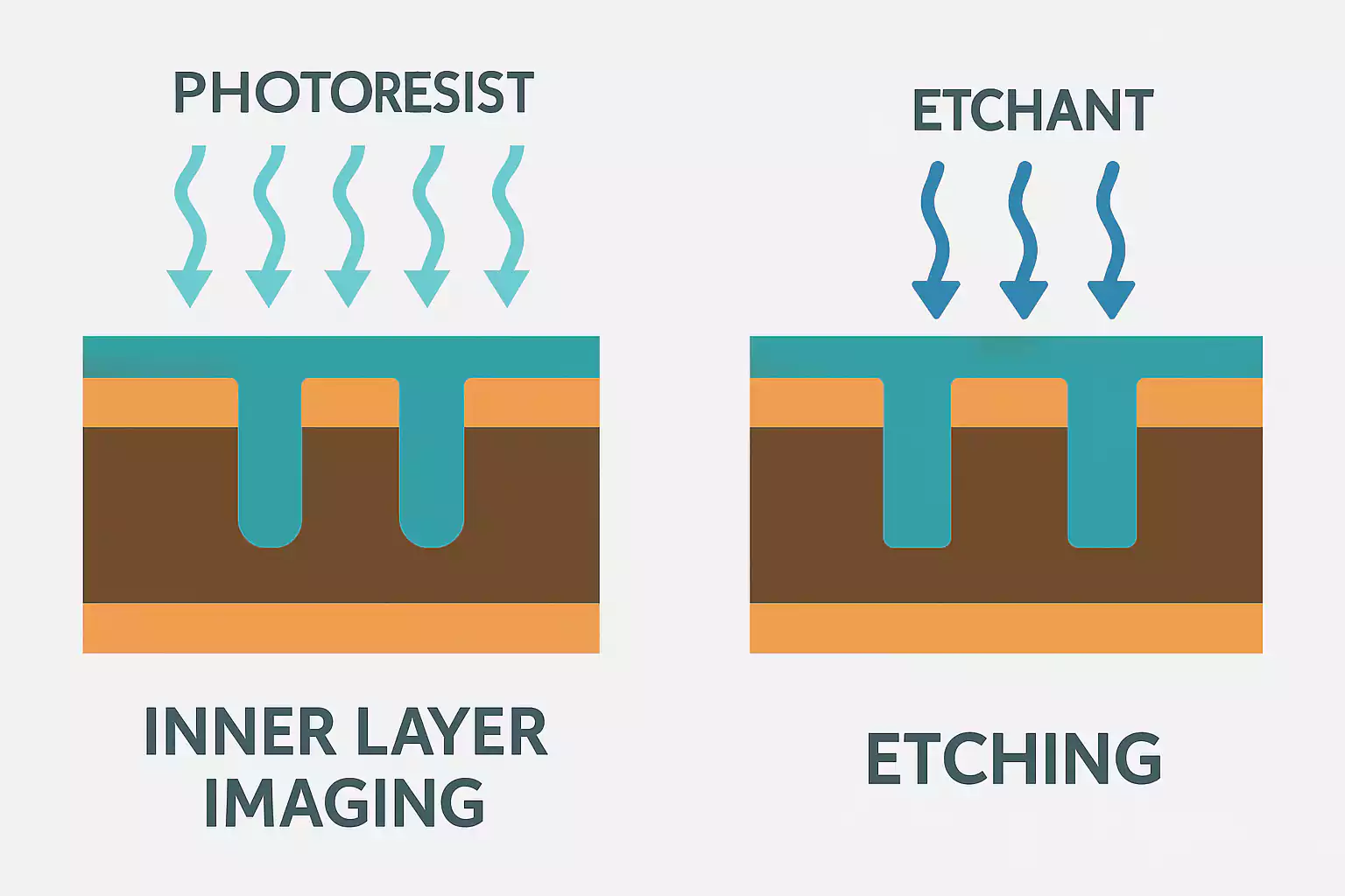
Inner-Layer Imaging and Etching
Inner layers define buried routing and reference planes before lamination.
- Imaging: Photoresist is laminated and patterned—ideally with LDI (Laser Direct Imaging) for tight alignment—then developed to reveal the desired copper features. Focus on artwork compensation for feature growth/shrink and precise layer-to-layer registration.
- Etching: Controlled etching removes exposed copper, forming traces. Etch rate depends on temperature, chemistry, and line speed; sidewall undercut must be accounted for in design rules and CAM compensation. After etch, AOI verifies geometry and defectivity before lamination.
- What to Watch: Over-etching thins traces and raises impedance; under-etching leaves copper whiskers. Cleanliness is vital—any debris or resist residue can become a reliability risk when trapped in the laminate.
Lamination
Lamination bonds inner layers using prepreg under heat and pressure to create a unified multilayer board.
- Resin Flow and Fill: Resin must flow enough to fill weave windows, etched cavities, and buried vias without starving adjacent areas. Excessive flow can shift features; insufficient flow risks voids and delamination.
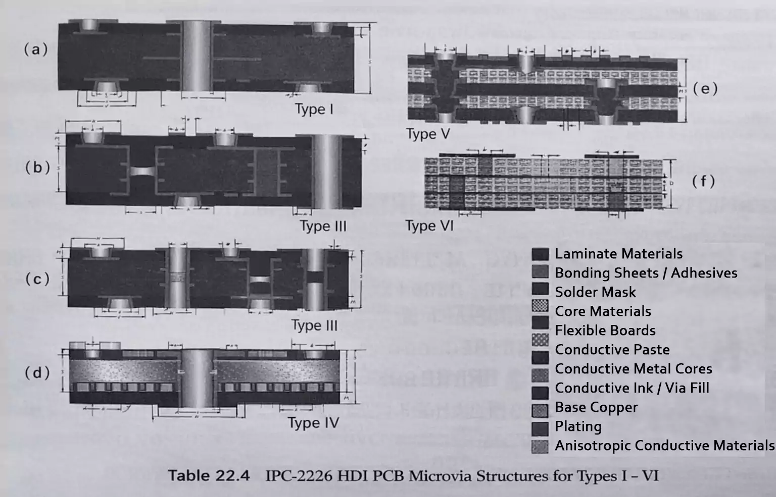
- Registration and Flatness: Press cycles, pinning methods, and tooling manage layer-to-layer alignment. Symmetrical constructions and balanced copper content help control Z-expansion and warpage. For HDI builds with multiple lam cycles, plan the order of microvia formation and buildup to ensure via reliability and coplanarity.
- Thermomechanical Considerations: Specify Tg and CTE appropriate for your assembly profile and service environment. High-Tg materials resist glass transition during reflow; matched CTE reduces stress on vias and pads.
Drilling and Via Strategy
Holes connect layers and anchor components; your via strategy impacts both manufacturability and testability.
- Hole Types:
• Through-holes are robust and cost-effective
• Blind/buried vias reduce layer transitions and free up routing
• Laser microvias enable HDI fan-outs, especially under fine-pitch BGAs (≤ 0.1 mm), and work best when stacked or staggered within tool limits - Process Controls: Mechanical drilling requires correct spindle speed and feed to limit smear and burring; entry/exit materials mitigate breakout. Laser drilling must balance energy to ablate resin without damaging copper. Maintain annular ring margins that reflect registration capability and final plating growth.
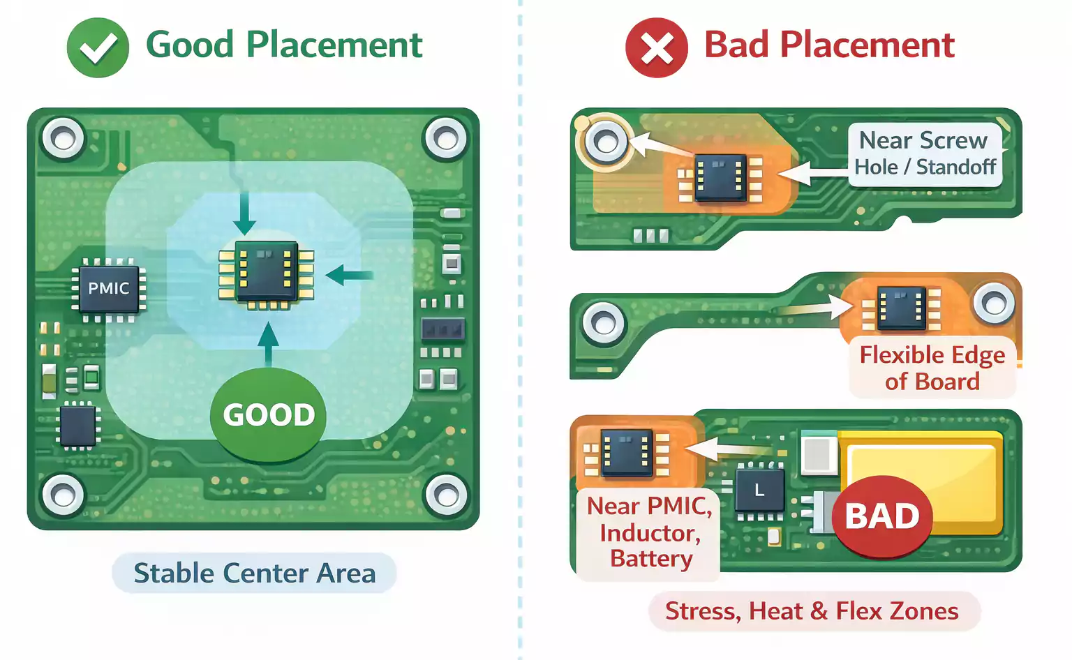
- Design Trade-Offs: Via-in-pad shortens escape length and improves SI/PI but requires copper filling and planarization to avoid solder voiding. Tenting or capping decisions affect cleaning, solderability, and test probe access. Decide these in DFM so the plating and mask processes are set accordingly.
PTH and Copper Plating
After drilling, hole walls are non-conductive. PTH (Plated Through Hole) processes create a conductive seed layer, then build up copper thickness.
- Sequence: Desmear/etchback prepares resin and glass; catalytic activation applies a palladium seed; electroless copper deposits a thin conductive layer. Electroplating increases copper in holes and on surfaces. Additive pattern plating can also build up pads and traces before final etch.
- Quality Metrics: Uniform copper thickness ensures thermal cycling reliability. Key controls include agitation, current density, throwing power, and electrolyte health. Microsections verify plating distribution and detect voids, cracks, or over-roughness that could hinder solderability.
- Risk Management: Watch for copper “dog-boning” at pad edges and localized high current density that produces nodules—both can compromise impedance and solderability.
Outer-Layer Patterning and Etching
Outer-layer imaging mirrors the inner-layer process but now must account for plated copper thickness and final impedance targets.
- Imaging and Pattern Plating: Dry film resist defines where copper should remain; pads and select traces may receive additional plating for robustness and wear resistance.
- Final Etch: Exposed copper is etched away, leaving finished conductor geometry. Because outer layers vary most due to plating growth, CAM compensation and controlled etch are crucial for accurate trace width and impedance.
- Defects to Prevent: Residues, over-plated nodules, and under-etched copper are detected by AOI—correct them here, as later steps will only magnify issues.
Solder Mask and Silkscreen
Solder mask preserves solderable features and protects everything else from oxidation and bridging.
- Mask Strategy: Define openings around pads with appropriate clearances; guard against slivers between fine-pitch pads by ensuring a minimum solder mask web. For BGAs, coordinate mask-defined versus copper-defined pads with your assembly house’s stencil and paste strategy. Set via treatments—tent, cap, or open—based on rework and testing needs.
- Cure and Registration: Proper exposure and thermal cure ensure adhesion and chemical resistance. Registration matters—misaligned mask can choke pads or expose copper to oxidation.
- Marking: Silkscreen (or laser marking) adds reference designators, polarity marks, and traceability codes. Keep ink off pads, maintain legibility under conformal coat, and place marks to survive depanelization.
Surface Finish Selection Guide
Surface finish bridges fabrication and assembly. Choose based on pitch, shelf life, and budget.
- HASL / Lead-free HASL: Durable and cost-effective; not as planar as other options. Suitable for moderate pitch, thicker boards, and rugged products.
- OSP (Organic Solderability Preservative): Very flat and economical; limited shelf life and reflow cycles. Ideal for high-volume SMT with short time-to-assembly.
- ENIG (Electroless Nickel Immersion Gold): Excellent planarity and corrosion resistance; ideal for fine-pitch, BGAs, and wire-bonding. Monitor for black-pad risk with solid process control.
- ENEPIG: Adds palladium for superior wire-bonding and gold thickness control; higher cost, premium reliability.
- Immersion Tin/Silver: Flat and solderable; requires careful handling and storage to prevent tarnish or intermetallic issues.
Match your finish to solder joint reliability needs, fine-pitch planarity, storage window, and cost per panel. For most advanced SMT, ENIG or ENEPIG is preferred; for cost-sensitive, fast-turn builds, OSP is effective if assembly is prompt.
Test, Inspection, and Design for Testability
Quality gates confirm continuity, isolation, and geometry before shipment.
- Electrical Test:
• Flying probe is flexible and fast for prototypes or variable mix; no fixture cost, lower throughput
• Bed-of-nails fixtures provide high speed and repeatability for volume, but require upfront fixture design and panel consistency - Optical/X-ray Inspection: AOI verifies trace/space conformity and mask registration; X-ray (if used pre-assembly) validates hole integrity or special buried features.
- Design for Test (DFT): Provide accessible test pads for nets that can’t be probed at component pins, maintain clearances for probe tips, and ensure your supplied netlist matches final CAM. For critical impedance, include coupons and acceptance bands for TDR verification.
Depanelization, Cleaning, and Packaging
Final steps protect your finished boards.
- Depanelization: Choose V-scoring for simple, linear separations and high density; use routed tabs for complex shapes or to protect edge-mounted components. Match keep-outs and copper pullbacks to your method.
- Cleaning: Remove ionic residues and particulates that could cause corrosion or solderability issues. Even boards sent directly to assembly benefit from controlled cleanliness and dry packaging.
- Packaging: Use moisture-barrier bags, desiccant, and humidity indicators as needed. Label with lot, date, and revision for traceability, and include handling guidelines—especially for OSP and immersion silver finishes.
Three Practical Scenarios and What to Choose
- Prototypes and Small Batches:
Prioritize speed and flexibility—use flying-probe test, ENIG or OSP finishes, and panelization for quick line changeovers. Keep design rules conservative unless HDI is essential for your application. - Mass Production and Cost Control:
Focus on panel utilization, repeatable depanel edges, and fixture-based electrical test for throughput. Choose a finish that fits takt time and storage—OSP for rapid assembly, lead-free HASL for ruggedness, ENIG for fine-pitch. Lock a stable stack-up early to ensure consistent impedance. - High-Speed/RF/HDI:
Specify low-loss materials with documented Dk/Df at your operating frequency, constrain copper roughness if insertion loss is critical, and define microvia strategy (stacked vs. staggered) with realistic aspect ratios. Use controlled impedance coupons and acceptance bands; confirm mask and finish compatibility for fine-pitch assembly.

Conclusion and Next Steps
A disciplined tecnograph PCB process turns design intent into reliable hardware: appropriate materials and stack-up, controlled imaging and etching, robust vias and plating, the right mask and finish, and a test plan tailored to the final application. When data is clear and tolerances are realistic from the start, yields improve, cycle times shrink, and costly late-stage rework is avoided.
If you’re ready to validate a design or lock in a stack-up, share your build files for a manufacturability review and a fast, accurate quote.