Introduction
Solder paste stencil printing is a vital step in modern surface mount technology (SMT) assembly. It involves applying solder paste onto a printed circuit board (PCB) through a precisely designed stencil to ensure accurate deposition on each pad. The quality of this process directly influences solder joint integrity, component placement accuracy, and overall product reliability.
This article offers a clear and comprehensive overview of solder paste stencil printing—from basic concepts and stencil design, to key printing parameters and common defects. You’ll also learn about cleaning and maintenance practices, as well as best practices for improving yield and reducing rework in SMT production.
Whether you’re an engineer optimizing a high-volume SMT line or a technician working on prototypes, this guide will help you understand and control the most important factors in stencil printing.
SMT Stencil Printing Process Overview
Solder paste stencil printing is the first and most crucial step in the SMT assembly process. It defines how accurately and consistently solder paste is deposited onto the surface mount pads of a PCB, which directly affects component placement and solder joint quality.
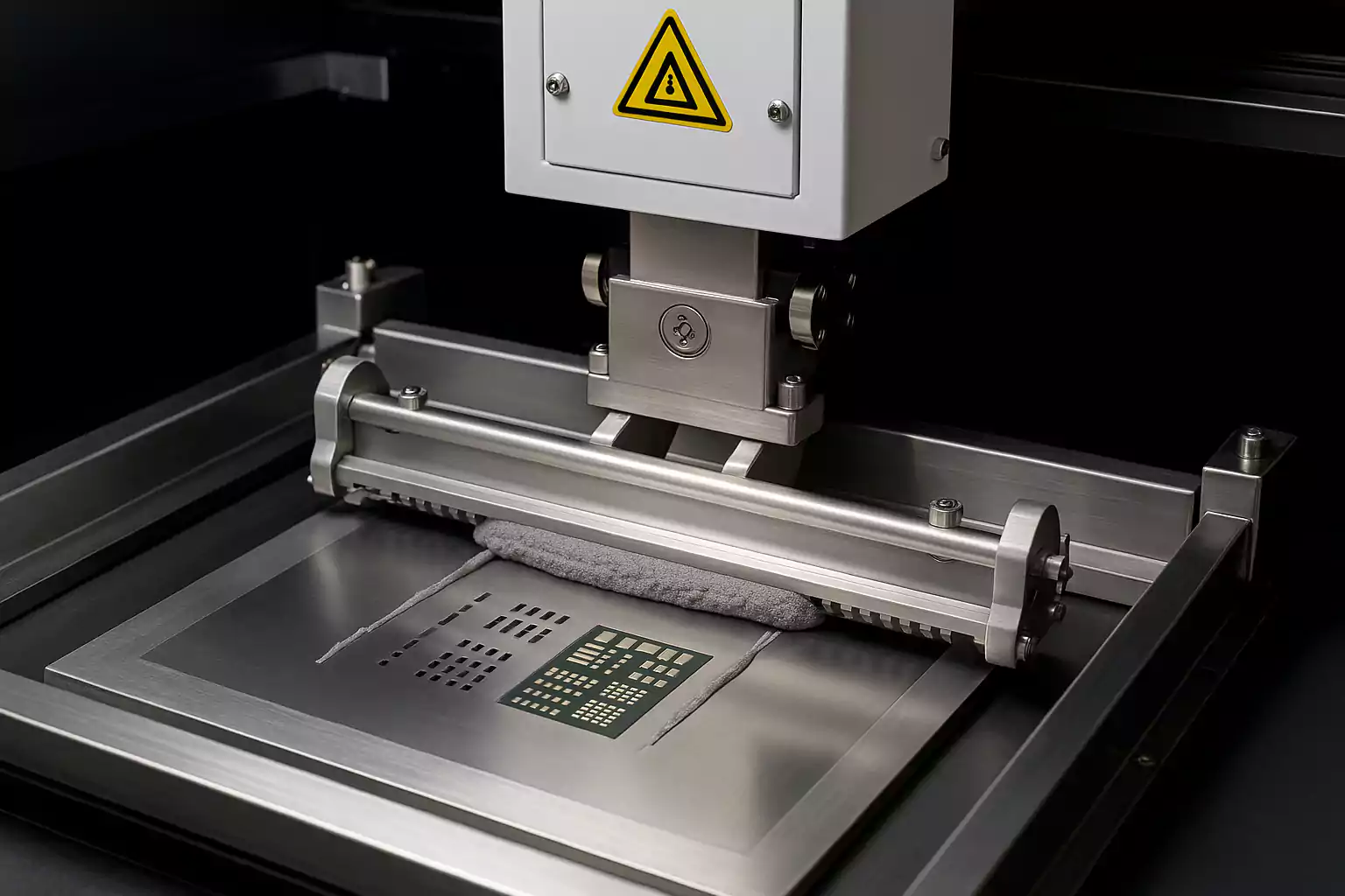
The typical stencil printing process involves the following key steps:
1. Stencil and PCB Alignment
Before printing begins, the stencil (usually made of stainless steel or nickel) is carefully aligned with the PCB. Fiducial marks on the board and alignment systems in the printer ensure precise positioning, especially for fine-pitch components.
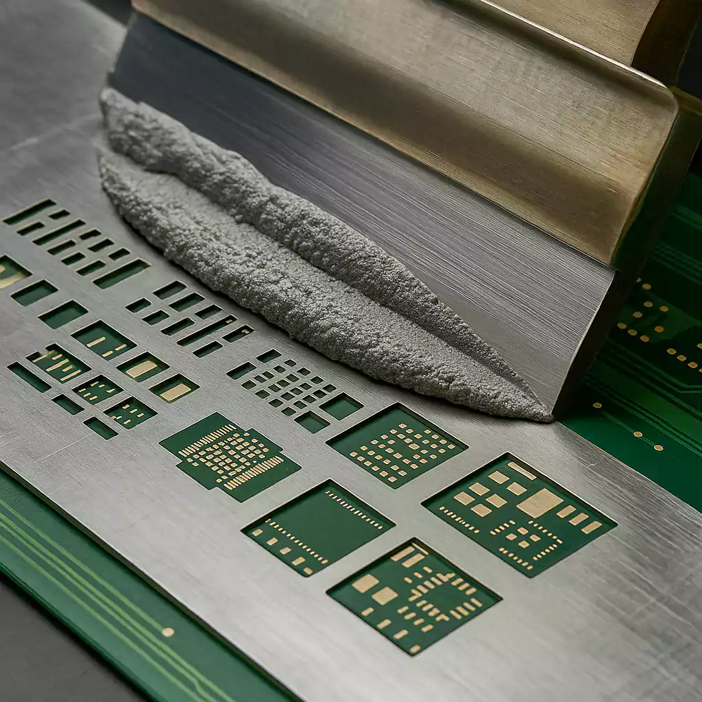
2. Solder Paste Application
A metal squeegee blade moves across the stencil, pushing solder paste into the stencil apertures. The paste fills the openings and deposits onto the PCB pads underneath. The squeegee’s speed, angle, and pressure are all critical parameters that determine the paste's uniformity and volume.
3. Snap-off or Separation
Once the solder paste is applied, the stencil is lifted (either with or without snap-off gap depending on the setup), leaving a clean deposit of solder paste on the PCB. Proper separation speed and stencil surface finish are essential to prevent smearing or bridging.
4. Post-Print Inspection
After printing, the board passes through solder paste inspection (SPI) systems to check for defects like insufficient volume, bridging, or misalignment. Early detection at this stage significantly reduces downstream rework.
5. PCB Transfer to Pick-and-Place
Clean and accurate solder paste deposits are now ready to receive components in the next step of the SMT process. The board is transferred to the pick-and-place machine either manually or via an inline conveyor system.
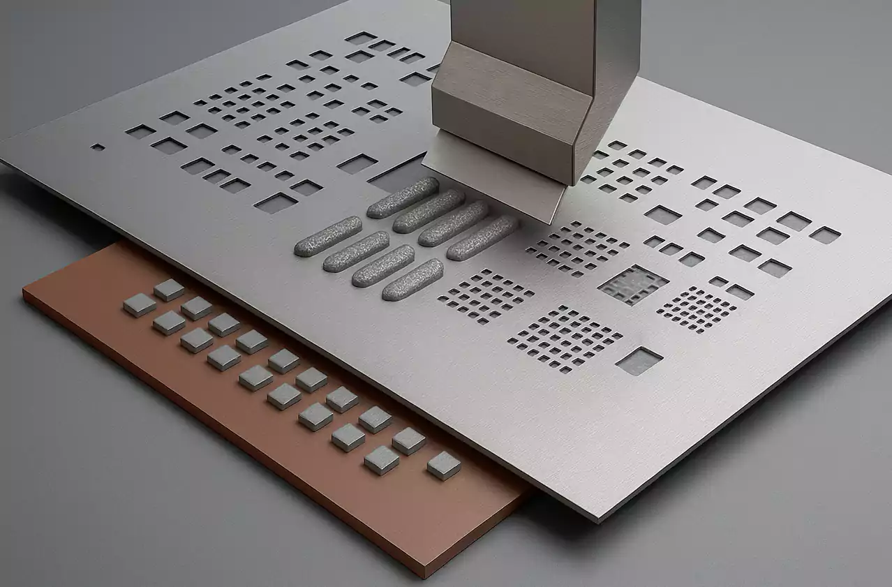
Stencil Design Fundamentals
The effectiveness of solder paste printing depends heavily on proper stencil design. A well-designed stencil ensures accurate paste volume, clean release, and consistent transfer to the PCB pads. Poor stencil design, on the other hand, can lead to insufficient solder, bridging, tombstoning, or poor component alignment.
Here are the core elements to consider when designing a stencil for SMT assembly:
1. Stencil Material Types
Most SMT stencils are made from stainless steel, electroformed nickel, or polyimide film. Each material has unique characteristics that affect durability, print definition, and cost.
| Material Type | Characteristics | Advantages | Typical Use Cases |
|---|---|---|---|
| Stainless Steel | Most common material; laser-cut | Durable, affordable, widely available | General SMT production |
| Electroformed Nickel | High-precision; smooth aperture walls | Best for fine-pitch components; excellent paste release | High-density interconnect (HDI), BGA, 01005 |
| Polyimide (Mylar) | Flexible, chemically etched or laser-cut | Low cost, fast turnaround (for prototypes) | Prototyping, low-volume applications |
2. Stencil Thickness Selection
Stencil thickness directly affects the volume of solder paste deposited. Thicker stencils deliver more paste, which is useful for large components or connectors, while thinner stencils are preferred for fine-pitch ICs.
| Stencil Thickness | Typical Pitch Range | Recommended For |
|---|---|---|
| 0.10 mm (4 mil) | ≤ 0.5 mm pitch | Fine-pitch QFP, BGA, CSP, 0201/01005 |
| 0.12 mm (5 mil) | 0.5–0.8 mm pitch | General-purpose SMT |
| 0.15 mm (6 mil) | ≥ 0.8 mm pitch | Large pads, connectors, through-hole paste-in-hole |
3. Aperture Design and Geometry
Proper aperture design ensures controlled paste volume and clean stencil release. The following aspects are critical:
- Aperture Reduction: It's standard to reduce aperture size by 10–20% (also called "shrinkage") to prevent bridging.
- Corner Radius: Rounded corners help with smoother paste release and reduce clogging.
- Aperture Shapes: Use home-plate or windowpane shapes for thermal pads or large exposed areas to avoid voids.
4. Area Ratio and Aspect Ratio
These two key ratios help determine whether solder paste will release cleanly from the stencil aperture.
- Area Ratio (AR) = (Aperture opening area) / (Aperture wall area)
- Recommended AR ≥ 0.66 for reliable release
- Aspect Ratio = (Aperture width) / (Stencil thickness)
- Recommended minimum: 1.5
If the area ratio is too low, solder paste may stick inside the aperture, causing insufficient or inconsistent deposits.
Summary Table: Stencil Design Best Practices
| Design Factor | Best Practice Recommendation |
|---|---|
| Material | Stainless steel for general use, nickel for fine-pitch |
| Thickness | 4–6 mil depending on pitch and component size |
| Aperture Reduction | 10–20% from pad size |
| Corner Design | Rounded for better release |
| Area Ratio | ≥ 0.66 |
| Aspect Ratio | ≥ 1.5 |
Printing Parameters and Their Impact
Controlling the key parameters in solder paste stencil printing is essential for achieving consistent, defect-free results. Improper settings can lead to a range of issues, including insufficient solder, smearing, and bridging. Below are the most critical printing parameters and their roles in the process:
Squeegee Speed
Squeegee speed determines how quickly solder paste is pushed across the stencil surface. A typical speed range is 20–50 mm/sec.
- Too fast: Incomplete aperture filling or paste smearing
- Too slow: Excess paste pressure, leading to stencil wear or uneven deposition
Squeegee Pressure
Squeegee pressure must be enough to wipe the stencil clean without deforming it or damaging the PCB.
- Recommended range: 0.5–1.5 kg per 25 mm of blade width
- Too low: Paste left on stencil surface
- Too high: Paste scooping, stencil damage, reduced stencil life
Squeegee Angle
Typical squeegee angles range from 45° to 60°.
- Lower angles provide better aperture filling (helpful for complex boards)
- Higher angles increase wipe efficiency but may reduce paste transfer
Snap-Off Distance (Separation Distance)
Snap-off distance refers to the gap between the stencil and PCB during printing (mainly relevant in semi-automatic/manual printers).
- Common setting: 0–0.5 mm, or zero-gap (contact printing) for modern equipment
Print Environment Conditions
Environmental control is often overlooked but plays a key role in paste behavior:
- Temperature: 22–28 °C (72–82 °F)
- Humidity: 40–60% RH
- Contamination: Keep stencil surface and surroundings clean to avoid defects
Stencil Cleaning Frequency
Regular cleaning between prints helps prevent blocked apertures and paste smearing.
- Clean every 5–10 boards depending on board complexity and paste type
Common Printing Defects and Troubleshooting
Even with a well-designed stencil and optimized print parameters, solder paste printing can still suffer from defects that negatively impact SMT assembly yield. Understanding these common issues—and how to quickly identify and fix them—is critical for maintaining high production quality.
Here’s an overview of typical printing defects, their root causes, and recommended solutions:
Common Solder Paste Printing Defects
| Defect | Possible Causes | Recommended Solutions |
|---|---|---|
| Insufficient Solder | Low paste volume due to small apertures, low area ratio, dry paste | Increase aperture size, check area ratio (>0.66), ensure paste is within shelf life |
| Bridging | Excess paste, poor aperture design, misalignment | Reduce aperture size, inspect stencil alignment, optimize squeegee pressure |
| Smearing | Paste leakage under stencil, incorrect snap-off or excessive paste | Use contact printing, clean stencil frequently, adjust snap-off distance |
| Misalignment | Poor board-to-stencil alignment, worn alignment pins | Calibrate alignment system, replace damaged tooling or pins |
| Aperture Clogging | Dry or high-viscosity paste, lack of stencil cleaning | Use fresh paste, reduce dwell time, increase cleaning frequency |
| Paste Slumping | Low viscosity or overly warm paste environment | Maintain ambient temp (22–28 °C), store paste properly before use |
| Voids in Pads | Large apertures, trapped air, poor paste release | Modify aperture design (e.g., windowpane or segmenting), consider step stencil |
Additional Troubleshooting Tips
- Always monitor SPI data (if available) for early detection of volume or shape anomalies.
- Perform print-to-inspect intervals every 5–10 boards, especially during setup.
- Track first-pass yield (FPY) trends to identify long-term stencil or process degradation.
Visual Inspection Aids
If your process does not include SPI equipment, use magnification tools to inspect:
- Paste height and coverage
- Clean aperture definition
- Consistency across pads
Stencil Cleaning and Maintenance Best Practices
Clean stencils are essential for consistent solder paste transfer and print quality. Residue buildup in apertures can lead to defects such as bridging, insufficient solder, and misprints. A proper cleaning routine minimizes downtime, reduces rework, and extends stencil lifespan.
Cleaning Methods
| Method | Use Case | Notes |
|---|---|---|
| Manual wipe | Prototyping, small batches | Use lint-free cloth and approved solvents |
| Ultrasonic cleaning | Clogged or fine-pitch stencils | Effective but requires controlled handling |
| Automated under-wipe | Inline high-volume printing | Ensures consistent bottom-side cleaning |
| Spray system (offline) | Batch cleaning between runs | Choose chemistry compatible with coatings |
Recommended Frequency
- Inline cleaning: Every 5–10 prints for fine-pitch or dense boards
- Offline cleaning: After each production run or before storage
Storage & Handling
- Store stencils flat in protective racks
- Avoid touching stencil surfaces directly
- Use covers to prevent contamination
- Label stencils for traceability
Quick Maintenance Checklist
- Apertures free of paste residue
- No mesh or frame damage
- Flatness within tolerance
- Clean and dry before storage
Well-maintained stencils ensure stable print performance, reduce variation, and support higher first-pass yields.
Best Practices for High-Yield Stencil Printing
Achieving consistent, high-quality solder paste printing requires more than just good equipment—it also depends on disciplined process control and proactive attention to detail. Below are practical strategies that help maintain high first-pass yield (FPY) and reduce costly rework or failures downstream.
1. Use Fiducials and Support Pins
Proper alignment is critical. Use fiducial marks on the PCB and ensure the stencil printer’s vision system is calibrated for accurate alignment.
Additionally, support pins or tooling blocks should be placed strategically to prevent board flex during printing.
2. Standardize Print Parameters
Maintain consistent squeegee speed, pressure, and angle throughout production. Any variation between batches or operators can lead to inconsistent paste volumes or smear defects. Document and lock in parameters through your MES or printer settings.
3. Optimize Paste Management
Only use solder paste within its shelf life and store it under recommended conditions (typically 2–10 °C). Let the paste acclimate to room temperature before use, and stir it uniformly before loading to ensure consistent viscosity.
4. Verify First Article Prints
Always inspect the first few boards after setup using a solder paste inspection (SPI) system or magnification. Verify aperture coverage, paste height, and alignment before proceeding with full production.
5. Implement Routine Cleaning
Establish a cleaning schedule based on board complexity and stencil condition. Use automatic under-stencil wiping during production, and clean thoroughly offline between runs.
6. Monitor Process Stability
Track key metrics such as SPI volume percentages, print defects per board, and FPY trends. Process drift can be caught early by reviewing this data regularly, allowing timely adjustments.
7. Train and Audit Operators
Ensure operators are trained on stencil handling, paste preparation, and printer setup. Periodic audits help reinforce best practices and uncover gaps in execution.
Frequently Asked Questions (FAQ)
How do I choose the right stencil thickness?
Stencil thickness depends on the component pitch and pad size. Fine-pitch ICs (≤0.5 mm) usually require 4–5 mil stencils, while larger components or connectors may use 6 mil or thicker. Mixed designs often benefit from step stencils.
Can one stencil be used for multiple PCB designs?
It is not recommended. Each PCB layout requires unique aperture sizes and pad alignments. Using one stencil for different boards often causes misalignment and inconsistent solder deposition.
What causes insufficient solder paste deposits?
Common causes include small aperture-to-thickness ratios, clogged stencil openings, or worn squeegee blades. Ensuring proper aperture design, regular cleaning, and correct printing pressure helps solve this issue.
How often should stencils be cleaned?
For fine-pitch and dense boards, cleaning is recommended every 5–10 prints. At a minimum, stencils should be cleaned after every production run and before storage to prevent dried paste and contamination.
Is manual stencil printing reliable for prototypes?
Yes, manual printing can work for small batches or prototypes. However, it is less consistent than automated printers and more prone to defects. For higher accuracy, semi-automatic or automatic printers are preferred.
Conclusion
Solder paste stencil printing is a critical step in SMT assembly, directly affecting solder joint quality and production yield. Achieving reliable results depends on three key factors: good stencil design, stable printing parameters, and proper maintenance.
By focusing on accurate alignment, controlled paste deposition, and regular stencil care, manufacturers can minimize defects and improve first-pass yield. As PCB designs become smaller and more complex, mastering stencil printing remains essential for ensuring consistent, high-quality assembly.