In SMT (Surface Mount Technology) processing, inspection is critical to ensuring high product quality and production efficiency. Various testing and inspection methods are used throughout the assembly process to detect defects early and maintain reliability. Below are the most common testing methods applied in SMT PCB assembly:
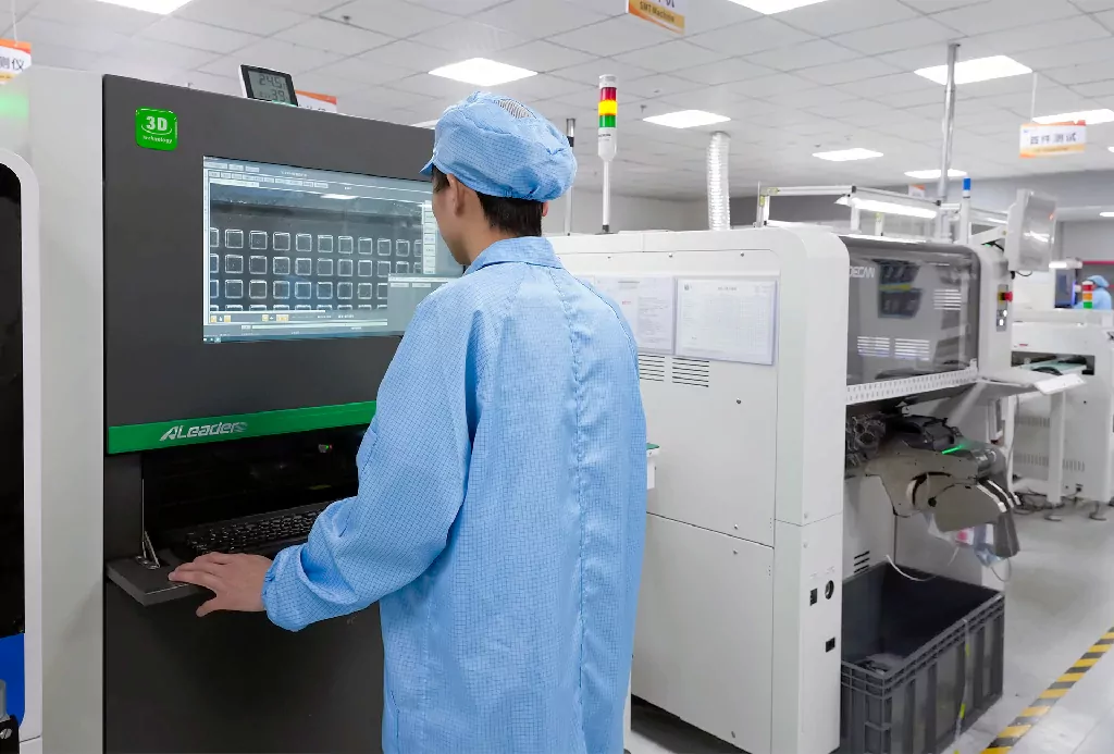
Visual Inspection
Visual inspection is the most fundamental method in SMT assembly. Using microscopes or intelligent visual systems, operators can detect assembly defects, misalignments, or soldering issues. Although simple, this step is crucial for catching visible errors before more advanced testing.
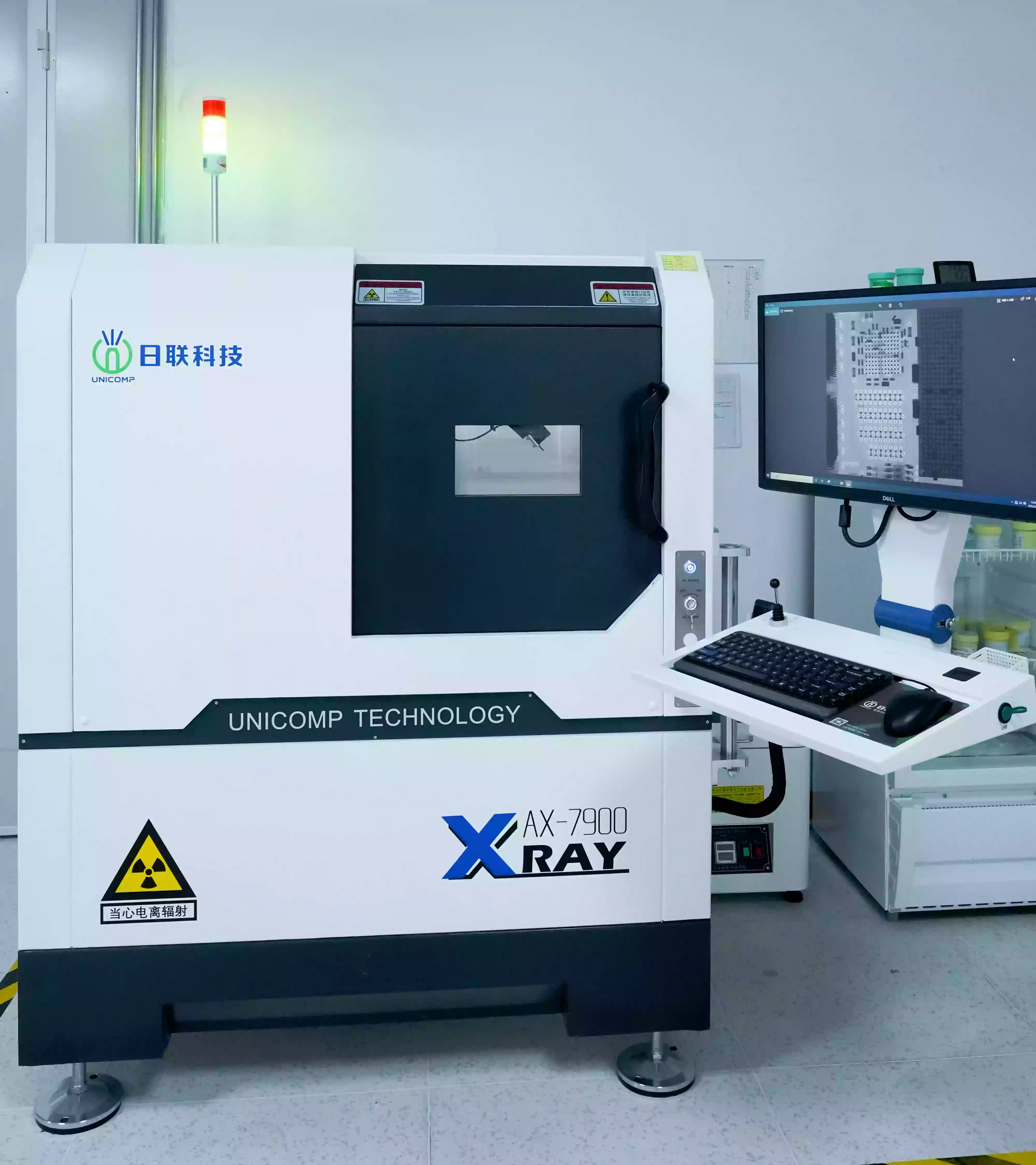
X-ray Inspection
X-ray testing allows manufacturers to inspect hidden solder joints and internal structures of the PCB without causing damage. This method is especially important for components like BGA (Ball Grid Array), where solder joints are not visible to the naked eye. X-ray inspection helps detect hidden defects such as voids, bridges, or cold solder joints.
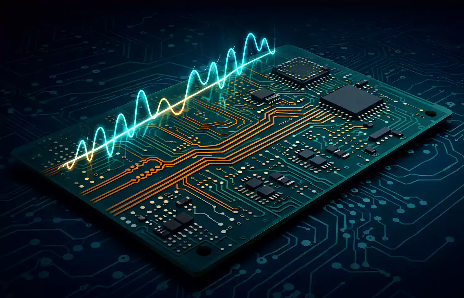
Infrared Inspection
Infrared inspection uses thermal imaging technology to monitor temperature changes during the soldering process. It helps identify overheating, cold solder joints, or thermal anomalies that may indicate potential defects, enabling timely corrective actions.
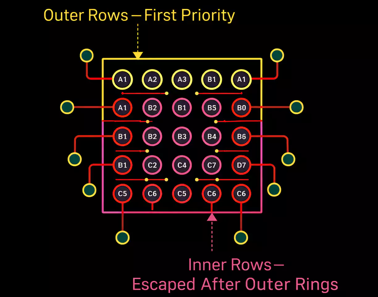
Automated Optical Inspection (AOI)
AOI uses high-resolution cameras and image processing software to inspect component placement, polarity, and solder joint quality. AOI systems can quickly and accurately detect missing components, misalignments, and soldering defects, significantly improving production line efficiency and quality control.
Solder Paste Inspection (SPI)
SPI focuses on inspecting the volume, height, and alignment of solder paste applied to the PCB before component placement. This ensures even distribution and proper application of solder paste, reducing the risk of soldering defects during reflow.
In-Circuit Test (ICT)
In-circuit testing verifies the electrical performance of components and circuits on the PCB. ICT checks for shorts, opens, resistance, capacitance, and other parameters, ensuring that the assembly meets electrical design requirements.
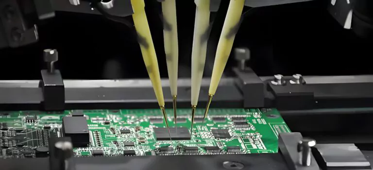
Flying Probe Test
The flying probe test is ideal for small-batch or prototype PCBs. It uses movable probes to test electrical connections and component functionality without the need for custom test fixtures, making it cost-effective for low-volume production.
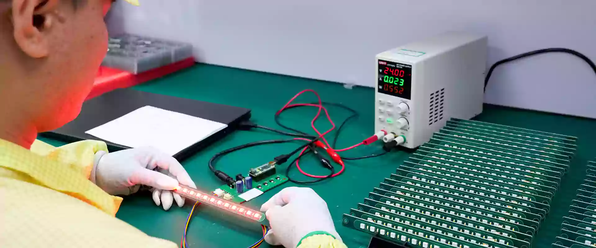
Functional Testing
Functional testing simulates the actual operating conditions of the electronic device to ensure it works as intended. This includes checking communication interfaces, signal integrity, and overall performance according to design specifications.
Environmental Testing
Environmental testing evaluates the durability and reliability of electronic products under extreme conditions. This may include temperature cycling, humidity exposure, vibration, and mechanical shock to ensure long-term stability in harsh environments.