


Introduction
Surface Mount Technology (SMT) has revolutionized electronics manufacturing by enabling ever-smaller, higher-performance circuit boards.
From the smartphones in our pockets to advanced automotive control units, SMT underpins the devices we rely on every day.
In this article, we'll demystify SMT—what it is, how it works, and why it matters—so that engineers, hobbyists, and decision-makers alike can confidently navigate its principles and applications.
By the end of this article, you will be able to:
- Clearly explain what SMT is and distinguish it from through-hole techniques
- Visualize the core process steps and understand how each contributes to board assembly
- Assess the pros and cons of SMT for your next project or manufacturing decision
- Identify key materials and equipment needed to set up or evaluate an SMT line
- Apply quality criteria to spot and prevent common SMT defects
With these insights in hand, let's dive into the world of Surface Mount Technology.
Basic Concepts & Definitions
What is SMT?
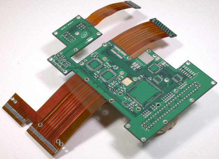
Surface Mount Technology (SMT) is a method of mounting electronic components directly onto the surface of a printed circuit board (PCB).
Instead of inserting component leads through drilled holes, SMT parts—known as Surface-Mount Devices (SMDs)—have flat terminations that are soldered onto metal pads.
This approach enables higher component density, faster automated assembly, and reduced manufacturing costs compared to older techniques.
SMT is one of the most common processes in modern PCB Assembly operations.Once all components are soldered and tested, the completed board is known as a PCBA.
SMT (Surface Mount Technology): A PCB assembly process in which components are placed and soldered directly onto board pads, without leaded insertion.
SMT vs. Through-Hole Technology (THT)
While SMT places components on the board surface, Through-Hole Technology (THT) requires component leads to pass through holes in the PCB and be soldered on the opposite side. THT offers stronger mechanical bonds—advantageous for heavy or high-stress parts—whereas SMT excels in miniaturization, speed, and cost efficiency.
Because SMT parts are smaller and assembly is largely automated, modern electronics—from smartphones to IoT sensors—rely heavily on SMT.
Key Terms & Abbreviations
- SMD (Surface-Mount Device): The components used in SMT, such as resistors, capacitors, and ICs, designed for surface mounting.
- PCB (Printed Circuit Board): A substrate of insulating material (typically fiberglass) with etched copper traces to electrically connect SMDs.
- Solder Paste: A mixture of solder powder and flux, applied to PCB pads before placing SMDs.
- Reflow Soldering: The process of heating solder paste to bond components to the PCB, typically in a reflow oven.
- Stencil: A thin metal mask used to accurately deposit solder paste onto PCB pads.
This solid foundation will help you appreciate each subsequent SMT process step and its role in modern electronics manufacturing.
History & Development
SMT's roots trace back to the 1960s, when engineers sought methods to replace bulky leaded components and manual insertion. Early solder-paste trials were promising but lacked reliable deposition and reflow control.
By the 1970s, pioneering pick-and-place machines could handle simple passive parts, but true scalability arrived in the 1980s with better paste, stencil, and oven technologies. This era saw SMT leap from niche prototyping into mainstream computer and telecom manufacturing.
The 1990s brought formalization: IPC standards codified best practices, and component vendors introduced fine-pitch packages—SOICs gave way to BGAs and LQFPs, multiplying circuit density.
In the 2000s, full automation—including inline inspection and real-time process feedback—transformed EMS factories. Today, SMT's evolution continues toward ever-smaller, more complex assemblies for IoT, automotive ADAS, and biomedical implants, driven by innovations in materials, machine vision, and data-driven process control.
References:
The development history of SMT surface technology
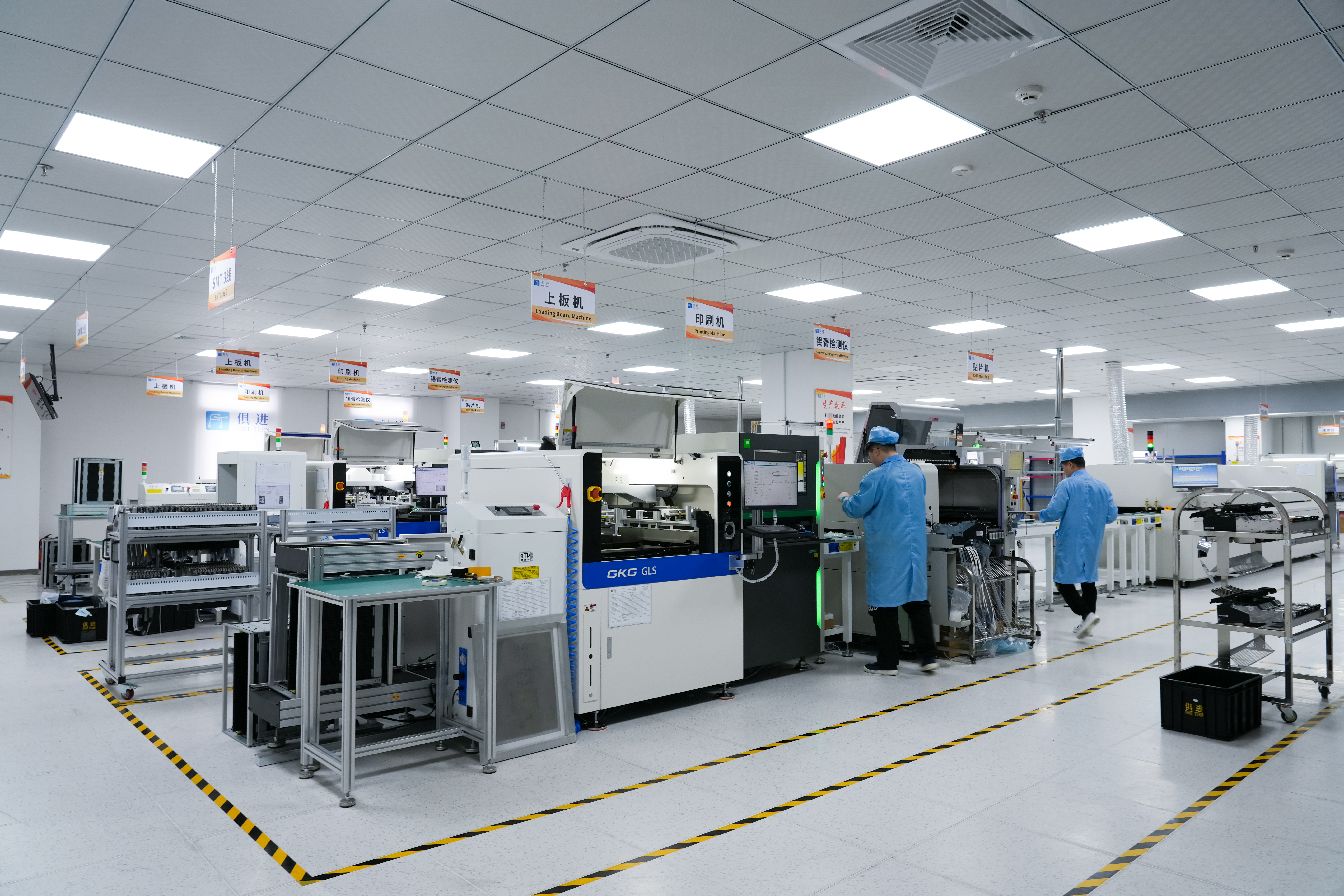
SMT Main Process & Workflow

1. Solder Paste Printing
Using a precision stencil, solder paste is deposited onto the PCB pads in one swift action.
- Stencil alignment: The PCB is registered under the metal mask via pins or vacuum.
- Paste application: A squeegee spreads solder paste across the stencil openings.
- Inspection: Optional SPI (Solder Paste Inspection) checks volume and placement before moving on.
2. Pick & Place
Automated machines pick components from reels or trays and place them onto the solder-pasted pads.
- Component feeding: Tape-and-reel or tray feeders supply parts to the head.
- Vision alignment: Camera system verifies component orientation and pad targets.
- High speed & accuracy: Modern heads achieve ±02 mm precision at thousands of placements per hour.
3. Reflow Soldering
Once components are positioned, the board travels through a controlled-temperature oven to melt the solder.
- Preheat zone: Gradually raises board temperature to activate flux without thermal shock.
- Soak zone: Holds at a moderate temperature to evenly heat all components.
- Reflow zone: Peaks above solder alloy liquidus to create metallurgical bonds.
- Cooling zone: Brings the assembly back to ambient, solidifying joints with minimal stress.
4. Cleaning & Post-Processing
Depending on flux type and end-use requirements, assemblies may undergo cleaning and further treatments.
- Flux residue removal: Aqueous or solvent cleaning removes ionic residues for high-reliability electronics.
- Conformal coating (optional): Protects boards from moisture, dust, and vibration in harsh environments.
5. Inline Inspection & Quality Control
To ensure defect-free production, several inspection methods are deployed either between or after process steps.
- SPI: Verifies solder paste deposition consistency before pick-and-
- AOI (Automated Optical Inspection): Checks component presence, polarity, and solder fillet quality on the line.
- X-Ray inspection: Reveals hidden defects in BGAs and other densely packed or under-component joints.
SMT Component Classification
| Category | Typical Examples | Primary Function |
| Passive Components | Resistors, Capacitors, Inductors | Voltage division, filtering, energy storage |
| Active Components | Diodes, Transistors, Integrated Circuits (ICs) | Signal amplification, switching, logic processing |
| Electromechanical Parts | Connectors, Relays, Switches | Board-to-board/field connections; mechanical actuation |
| Specialized Devices | Thermistors, Temperature/Humidity Sensors, Crystals | Environmental sensing; precise timing and reference |
Passive parts—like resistors and caps—don't introduce gain but shape voltage and current. Active devices (e.g. diodes, transistors, microcontrollers) perform logic, switching, and amplification.
Electromechanical items handle mechanical interfaces or isolation, while specialized devices cover sensing and timing functions essential in applications from temperature monitoring to clock generation.
Advantages & Limitations
Surface Mount Technology delivers significant benefits for modern electronics manufacturing, but it also poses specific challenges.
Below is a balanced look at both sides.
1. Advantages
- High Assembly Density
Small, flat SMT parts allow more components per square centimeter, enabling compact designs and multilayer boards.
- Faster Production Rates
Automated pick-and-place and reflow lines handle thousands of placements per hour, reducing cycle times.
- Cost Efficiency
Lower labor requirements and reduced material use (smaller components, no drilled holes) translate to lower per-unit costs at volume.
- Improved Electrical Performance
Shorter interconnects decrease parasitic inductance and capacitance, enhancing signal integrity for high-speed circuits.
- Consistency & Reliability
Automated processes minimize human error, yielding uniform solder joints and repeatable quality.
2. Limitations
- Precision Requirements
Tight placement tolerances (often ±0.02 mm) demand well-maintained equipment and precise calibration.
- Difficult Rework
Small pad sizes and close spacing make manual repair of mis-placed or defective parts more time-consuming and error-prone.
- Equipment Investment
High-speed pick-and-place machines, reflow ovens, and inspection systems require significant upfront capital.
- Thermal Stress Risks
Rapid heating and cooling in reflow can induce board warpage or component cracking if profiles are not carefully controlled.
- Component Availability
Some specialized or legacy parts may not be offered in surface-mount packages, requiring adapter boards or hybrid assembly.
Materials & Equipment Overview
Surface-mount assembly relies on a precise combination of consumables and machinery. High-quality solder paste, stencils, placement heads, and thermal profiling all work in concert to ensure reliable joints at high throughputs.
Below is an introduction to each critical material and piece of equipment you'll encounter on an SMT line:
Solder Paste & Flux
- Composition: A blend of fine solder powder (typically Sn-Ag-Cu alloy) and flux agents
- Function: Flux cleans oxides and promotes wetting; solder powder forms the metallurgical bond
- Key parameters:
- Alloy type: Lead-free (e.g., SAC305) vs. tin-lead (Sn63Pb37)
- Particle size: Ranges from Type 3 (25–45 µm) to Type 5 (15–25 µm) depending on stencil aperture and pitch
- Flux activity: No-clean vs. water-soluble vs. rosin
Stencils & Screen Printers
- Stencil: A thin stainless-steel or nickel mask with laser-cut apertures matching PCB pad patterns
- Screen printer: Machine that holds the stencil in precise alignment and uses a squeegee to deposit solder paste
- Important factors:
- Aperture quality: Sharp walls and accurate thickness (typically 0.1–15 mm) ensure consistent paste release
- Printer features: Pneumatic vs. mechanical squeegee, vision-assisted alignment, automatic stencil cleaning
Pick-and-Place Machines
- Purpose: Automatically pick components from tape/reel or trays and place them onto solder-pasted pads
- Critical specs: Placement accuracy (±01–0.05 mm), feeder capacity, vision-system resolution
- Types:
- High-speed chip shooters: Optimized for small passives (resistors, capacitors) at >100,000 CPH (components per hour)
- Flexible placement heads: Handle larger ICs, connectors, and odd-form parts with multi-tool changers
Reflow Ovens
- Function: Heat the board through a programmed thermal profile to melt solder and form reliable joints
- Zones: Typically 4–8 zones (preheat, soak, reflow peak, cooling) for precise temperature control
- Key considerations:
- Conveyor speed: Adjustable to match thermal profiles and throughput requirements
- Nitrogen option: Inert atmosphere reduces oxidation, improving solder quality for high-reliability assemblies
Inspection & Quality Equipment
- SPI (Solder Paste Inspection): Verifies paste volume and placement before component placement
- AOI (Automated Optical Inspection): Detects missing, misaligned, or defective solder joints and components
- X-Ray Inspection: Examines hidden joints under BGAs and multi-layer components for voids or bridges
- Other tools:
- Manual microscopes: For spot checks and rework
- Thermal profilers: To validate reflow oven profiles with thermocouples
Quality Control & Standards
Quality in SMT assembly hinges on both adhering to industry best practices and monitoring critical metrics to catch defects early. Below are the key standards, measurements, and defect-acceptance criteria that ensure reliable, high-yield production.
IPC International Standards Overview
| Standard | Scope & Focus |
| IPC 6012 | Qualification and performance specifications for rigid PCBs, including surface mount requirements. |
| IPC 610 | Acceptability of electronic assemblies—defines workmanship standards for solder joints, component placement, and cleanliness. |
| IPC 7525 | Stencil design guidelines to optimize solder paste volume and reduce printing defects. |
| IPC 7095 | Design and assembly of BGAs and other fine pitch devices, covering solder joint reliability and X ray inspection. |
| Importance | Aligns your process with globally recognized benchmarks, simplifies audits, and reduces field failures. |
Key Quality Metrics
| Metric | Definition & Target |
| Solder Paste Deposit Volume | Measured via SPI; typical tolerance ±10% of nominal volume (mg/mm²). |
| Placed Part Accuracy | X/Y positioning accuracy within ±0.03 mm for 0.5 mm pitch devices (camera verified). |
| Reflow Profile ΔT | Peak–soak temperature difference within ±5 °C to prevent tombstoning or voids. |
| First Pass Yield (FPY) | Percentage of boards passing inspection without rework—aim for ≥98% in mature lines. |
| Void Rate | Percentage of solder joint cross section voids; acceptable levels vary (e.g., ≤10% for BGA). |
Common Defects & Acceptance Criteria
- Solder Bridges: Unwanted connections between adjacent pads; classified as “major” if they short active nets (reject).
- Insufficient Wetting: Poor fillet formation or balling; judged by IPC-610 minimum fillet height (≥75% of component lead height).
- Tombstoning: One end of a passive device lifts off pad; any occurrence on a critical net requires rework.
- Mis-alignment: Component offset beyond IPC-610 tolerance zones (usually 25–50% of pad length).
- Void Formation: Internal air pockets in solder joints; inspected by X-ray and compared against IPC-7095 limits.
Adopting these standards and metrics—and routinely measuring them—creates a robust quality-control framework that catches assembly issues before boards ship to customers.
Applications
Consumer Electronics
From smartphones and tablets to wearables and home appliances, consumer devices demand ever-smaller form factors and rapid time-to-market. SMT's ability to densely pack components on multilayer PCBs makes it the backbone of modern handheld gadgets.
Automated lines spin up millions of boards per day, ensuring both consistent quality and the cost efficiencies needed in competitive retail markets.
Automotive Electronics
Advanced Driver-Assistance Systems (ADAS), infotainment clusters, and electric-vehicle power modules all rely on robust, high-reliability assemblies. SMT processes, combined with conformal coatings and rigorous thermal cycling tests, deliver the mechanical stability and signal integrity that automotive applications require.
As vehicles become ever more software-defined, SMT's flexibility to handle mixed assemblies—from tiny sensors to power MOSFETs—becomes a critical enabler.
Communication Equipment
Base stations, routers, and data-center switches push signal frequencies higher and bandwidths wider every year. Short interconnect lengths afforded by SMT minimize parasitic effects, improving high-speed signal integrity and reducing electromagnetic interference.
Moreover, SMT's rapid changeover capability allows OEMs to adapt quickly to evolving standards—from 5G radios to edge-computing modules—without costly tooling delays.
Medical & Aerospace
In life-critical and harsh-environment contexts, failure is not an option. SMT's precise control over solder quality, combined with advanced X-ray inspection and strict IPC-7095 guidelines, yields the uniformity and reliability demanded by implantable devices, diagnostic instruments, and avionics modules.
The technology also supports the miniaturization of wearable health monitors and flight-control sensors, where board real estate and weight are at a premium.
FAQs
What's the difference between SMT and SMD?
SMT (Surface Mount Technology) is the assembly process; SMD (Surface-Mount Device) refers to the individual components designed for SMT.
In other words, SMT is how you place and solder the parts, and SMDs are the parts themselves.
Recommended: SMD vs SMT
Why should I choose SMT over through-hole assembly?
SMT enables higher component density, faster automated throughput, and lower per-unit costs at volume. It also improves electrical performance by reducing lead inductance and capacitance.
Through-hole remains stronger mechanically, but SMT is generally preferred for modern, miniaturized designs.
Can SMT-assembled boards be reworked if there's a defect?
Yes, but rework requires specialized tools — hot-air stations, fine-tip soldering irons, and high-magnification inspection.
Small pad sizes and tight pitches make manual repair more challenging compared to through-hole, so it's best to minimize defects with robust process control.
How do I get started with SMT as a hobbyist or small-batch producer?
Begin by investing in a basic stencil printer, a benchtop pick-and-place (or even tweezers for simple boards), and a desktop reflow oven or hot-plate.
Start with Type 4 solder paste and 0805 passives before moving to fine-pitch ICs. Practice alignment on low-cost "practice" PCBs to build your skills.
Are there components not available in surface-mount packages?
A small number of large or legacy parts (e.g., certain power transformers, high-voltage connectors) may only come in through-hole packages.
In those cases, you can use hybrid assembly (mixing SMT and THT) or adapter boards that convert through-hole footprints to SMD pads.
How critical is stencil design for solder-paste printing?
Answer: Extremely. Aperture size, shape, and placement directly affect paste volume and transfer efficiency.
Poor stencil design leads to insufficient or excessive paste, causing tombstoning, bridges, or open joints. Always follow IPC-guidelines when creating or specifying your stencil.
What inspection methods should I use to ensure high yield?
1. SPI (Solder Paste Inspection): Verifies correct paste volume and alignment.
2. AOI (Automated Optical Inspection): Detects missing, misaligned, or bridged components post-reflow.
3. X-Ray Inspection: Uncovers hidden defects in BGAs and under-component joints.