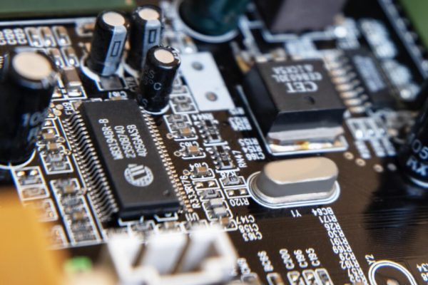
The electronics we carry every day—from smartwatches to EV-power modules—are possible largely because of one manufacturing leap: the surface-mount device (SMD).
By allowing parts to be placed directly on the surface of a printed-circuit board (PCB), SMD technology condensed entire radios, computers, and sensors into pocket-sized form factors.
Introduction
1. The Evolution of Electronic Assembly
Electronic assembly has progressed through three major eras. In the through-hole era (late 1950 s – 1970 s), bulky leads passed through drilled holes, enabling reliable but space-hungry boards.
The mixed-technology phase of the early 1980 s combined through-hole power components with emerging surface parts, laying the groundwork for full surface-mount adoption.
By the 1990 s, rising demand for lighter consumer devices, automated high-volume production, and finer signal integrity ushered in the surface-mount age, where almost every passive and active component is now available in miniature, lead-less packages.
2. SMD vs SMT – Quick Glossary
- Surface-Mount Device (SMD): an individual electronic component designed with metal terminations that can be soldered directly onto the surface of a printed-circuit board (PCB) without leads passing through the board.
- Surface-Mount Technology (SMT): the entire set of manufacturing processes (paste printing, pick-and-place, reflow soldering, inspection, rework) that enables reliable attachment of SMDs.
Put simply, SMD is the component; SMT is the process. For a deeper comparison—including historical milestones, process flow diagrams, and reliability metrics—see our dedicated guide: SMD and SMT - What You Need To Know.
3. Why SMD Is Displacing Through-Hole Assembly
3.1 Size and Weight Advantages
SMD packages such as 0402 resistors (1.0 mm × 0.5 mm) and WLCSP ICs eliminate long leads, trimming component footprints by up to 70% and reducing weight dramatically—critical for smartphones, wearables, and aerospace payloads.
3.2 Automation and Cost Efficiency
Modern pick-and-place machines routinely deposit 70,000+ components per hour, far surpassing manual insertion rates. Combined with stencil solder-paste printing and convection reflow, SMT slashes labor costs and supports just-in-time production with minimal human intervention.
3.3 Design Freedom and Electrical Performance
Shorter interconnects lower parasitic inductance and capacitance, enabling cleaner high-frequency signals, faster edge rates, and improved EMC performance. Designers also gain board-area savings for additional circuitry or battery capacity—key in today’s IoT and EV applications.
SMD / SMT / Through-Hole — Comprehensive Comparison
1. Manufacturing Workflow: Placement vs. Insertion
SMT line-flow begins with stencil solder-paste printing, followed by high-speed pick-and-place machines and convection reflow. We utilize advanced 16‑nozzle SMT machines capable of placing tens of thousands of components per hour, ensuring the stable production of high‑quality, high‑density PCB assemblies.
Through-hole (THT) still dominates large connectors, power parts, and harsh-vibration products. Components are manually or semi-automatically inserted, then soldered en-masse by wave solder or selective dip. Even semi-automated lines often finish only 100–500 boards per day, so labor cost per board is an order of magnitude higher than SMT at scale.
Bottom line: for high-volume, fine-pitch designs, SMD + SMT wins on speed and cost; THT remains valuable where mechanical strength or high current trumps density.
2. PCB Design Requirements
| Requirement | SMD / SMT | Through-Hole |
|---|---|---|
| Land pattern | Flat pads sized per IPC-7351 (Nominal, Least, Most) with solder-mask-defined or copper-defined outlines. | Plated through-holes; drill diameter = lead Ø + 0.2–0.3 mm; annular ring ≥ 0.25 mm. |
| Layer stack impact | No drill hits → easier HDI routings, microvias, buried/blind vias. | Hole barrels eat inner-layer real estate; dense designs demand via-in-pad or staggering tricks. |
| Thermal relief | Small pads dissipate less heat—critical for lead-free reflow. | Large copper planes require spoke-style reliefs to prevent cold joints during wave. |
3. Soldering Methods & Common Defects
3.1 Reflow Soldering (SMT)
A standard lead-free profile features:
- Pre-heat/Soak: 150 – 180 °C for 60–120 s to activate flux.
- Ramp to Peak: 230 – 245 °C, with coldest joint > 235 °C for Sn-Ag-Cu alloys.
- Cool-down: ≤ 4°C/s to minimize micro-cracks.
Typical SMT defects & mitigations:
| Defect | Root Cause | Mitigation |
|---|---|---|
| Tombstoning (chip stands up) | Uneven wetting forces on tiny 0402 pads | Symmetric stencil apertures, slower ramp rate |
| Voids in BGA | Excess paste, trapped volatiles | Reduce aperture area ratio, tweak soak time |
| Solder Balls | Paste spatter | Lower peak, adjust stencil release |
3.2 Wave / Selective Wave Soldering (THT & Mixed)
Boards glide over a molten wave at 245 – 265 °C; fluxing and pre-heat ensure hole wetting. Selective pallets or mini-waves let designers keep fine-pitch SMDs on the same board without masking.
Common THT defects include icicles, bridging, and pad lifting—usually tied to improper pre-heat or excessive conveyor speed.
4. Reliability & Test Cost Considerations
- Mechanical robustness: THT leads anchor deep into the board, resisting pull-out and vibration—ideal for transformers or high-current pins. SMD joints are mechanically weaker but gain reinforcement from conformal coat or under-fill on BGA/CSP packages.
- Thermal cycling: Shorter SMD interconnects lower CTE mismatch stress; however, very small solder volumes are more sensitive to void-induced fatigue.
- Test strategy: Dense SMT boards rely on flying-probe or boundary-scan; fixtureless setups cut NRE. THT often uses bed-of-nails ICT—excellent coverage but high fixture cost and long lead time.
5. Where Each Technique Excels
- Pure SMT (SMD components): smartphones, laptops, IoT sensors, automotive ADAS—where size, weight, and RF integrity matter.
- Pure THT: industrial controls, high-voltage power supplies, military connectors—where stress or current demands outweigh density.
- Mixed Technology: consumer AC adapters, LED lighting boards, aerospace avionics—SMT for logic & passives, THT for large electrolytics or edge connectors.
SMD Components Overview
Surface Mount Devices (SMDs) represent the cornerstone of modern electronics manufacturing, allowing for compact, high-speed, and automated PCB assembly. Understanding the major types of SMD components not only helps in effective circuit design but also ensures better sourcing and reliability.
Below is a categorized overview of the most common SMD components used in today's electronics industry.
1. Passive Components
Passive components do not generate energy but influence the flow of electrical current. They are foundational in filtering, timing, and impedance control across virtually all circuit types.
Resistors come in thick film, thin film, and alloy shunt types. Thick film resistors are widely used due to their affordability and reliability in general-purpose circuits, while thin film resistors offer greater precision and stability for sensitive analog and measurement systems. Alloy shunt resistors provide ultra-low resistance and are commonly applied in current sensing for power electronics.
Capacitors are available in multiple formats, such as MLCC (Multilayer Ceramic Capacitor), tantalum, and aluminum electrolytic. MLCCs dominate due to their compact size, high-frequency performance, and affordability. Tantalum capacitors provide stable capacitance in small packages, whereas electrolytic types are chosen for high capacitance requirements in power supply filtering.
Inductors and ferrite beads are crucial for electromagnetic interference (EMI) suppression and energy storage in power conversion circuits. Ferrite beads are especially valuable in filtering high-frequency noise on power lines, while chip inductors are key in RF circuits and voltage regulation stages.
2. Active / Semiconductor Components
Active components are essential for signal amplification, voltage regulation, and digital logic implementation. These parts play a critical role in enabling smart, programmable, and high-performance circuits.
Diodes used in SMD formats include standard rectifiers, Schottky diodes, and ESD protection diodes. Schottky diodes are favored for their low forward voltage and fast switching, improving energy efficiency in power applications.
ESD diodes protect sensitive ICs from voltage transients in USB, HDMI, and other high-speed interfaces.
Transistors,including BJTs (Bipolar Junction Transistors), MOSFETs, and IGBTs, serve as the building blocks for amplification and switching. BJTs are suited for analog signal control, while MOSFETs are standard in switching power supplies, battery management, and motor drivers.
IGBTs combine high-voltage capability with fast switching, making them ideal for industrial motor control and high-power inverters.
Integrated Circuits (ICs) in SMD packaging such as QFN (Quad Flat No-lead), BGA (Ball Grid Array), and WLCSP (Wafer Level Chip Scale Package) encapsulate complex functionalities—from microcontrollers and memory to RF modules and sensors—within minimal footprint.
QFN is widely used in space-constrained designs, BGA enables high-density interconnections for processors, and WLCSP supports ultra-compact applications like smartphones and wearables.
2. Electromechanical Components & Miscellaneous Devices
This category includes components that bridge electrical and mechanical functions, or add intelligence through sensing and timing features.
Crystals and oscillators provide precise timing signals necessary for synchronous data transmission and microprocessor operation.
Quartz crystals offer high frequency stability, while MEMS-based oscillators are increasingly popular for rugged and compact timing applications in portable electronics.
Connectors, switches, and LEDs in SMD formats contribute to human interfaces, system interconnections, and visual feedback. SMD tactile switches are common in user panels and control devices. SMD LEDs offer low-power lighting, used in indicators, displays, and backlights.
MEMS sensors and other transducers are integral to the evolution of smart electronics and the Internet of Things (IoT). MEMS devices like accelerometers, gyroscopes, and microphones offer compact sensing with digital interfaces.
Environmental sensors for temperature, humidity, air quality, and pressure enable intelligent monitoring in smartphones, wearables, industrial automation, and smart homes.
Package Sizes and Marking Code Quick Reference
Surface Mount Devices (SMDs) are categorized not only by their function but also by their physical package size and identification codes. Understanding these parameters is essential for PCB layout, component selection, manufacturing compatibility, and inventory management.
This section provides a comprehensive guide to interpreting SMD package sizes and component marking systems.
1. Imperial ↔ Metric Package Size Conversion Chart
SMD components are typically identified by standard package size codes in both imperial and metric formats. These codes define the length and width of the component in hundredths of inches (imperial) or in tenths of millimeters (metric). Here's a conversion chart for the most commonly used sizes:
| Imperial Code | Metric Code | Dimensions (mm) | Common Applications |
|---|---|---|---|
| 01005 | 0402 | 0.4 × 0.2 | Ultra-compact IoT, hearing aids |
| 0201 | 0603 | 0.6 × 0.3 | Wearables, compact mobile circuits |
| 0402 | 1005 | 1.0 × 0.5 | Smartphones, high-density PCBs |
| 0603 | 1608 | 1.6 × 0.8 | General-purpose electronics |
| 0805 | 2012 | 2.0 × 1.25 | Power supply filtering, signal bypassing |
| 1206 | 3216 | 3.2 × 1.6 | LED drivers, high-power resistors |
| 1210 | 3225 | 3.2 × 2.5 | Tantalum capacitors, automotive applications |
| 1812 | 4532 | 4.5 × 3.2 | Surge protection, power filtering |
| 2220 | 5650 | 5.6 × 5.0 | Industrial, high-voltage environments |
Tip: Always verify actual dimensions in the manufacturer's datasheet—package codes may vary slightly between manufacturers.
2. SMD Resistor and Capacitor Marking Code System
Due to limited space on tiny SMD packages, value markings use concise numerical and alphanumerical codes. Here's how to decode them:
Resistor Marking Codes
SMD resistors commonly use 3-digit or 4-digit numerical codes:
| Code Type | Example | Interpretation |
|---|---|---|
| 3-digit | 103 | 10 × 10³ = 10 kΩ |
| 4-digit | 4702 | 470 × 10² = 47 kΩ |
| "R" Format | 4R7 | 4.7 Ω (R = decimal) |
- 3-digit format is standard for resistors from 1 Ω to 999 kΩ
- 4-digit format is common in 1% or precision resistors
- Values under 10 Ω often use the "R" format
Capacitor Marking Codes
Most ceramic capacitors (MLCC) under size 0603 are unmarked. For those with markings:
104= 10 × 10⁴ pF = 0.1 μF471= 47 × 10¹ pF = 470 pF
Tolerance Letter Codes (Capacitors):
| Code | Tolerance |
|---|---|
| J | ±5% |
| K | ±10% |
| M | ±20% |
Note: Always cross-reference component codes with tape/reel packaging or supplier datasheets, especially for small-value capacitors or unmarked parts.
References / Verified Sources:
Murata Manufacturing – MLCC Size & Marking
Digi-Key Package Size Reference Table
Vishay Resistor Marking Standards
JEDEC Outline Standard MO Series
Selection, Design, and Soldering in Practice
Selecting and designing with Surface Mount Devices (SMDs) goes beyond datasheet specifications. Real-world success depends on proper component selection, PCB pad design, soldering parameters, and post-process inspection. This section offers a practical, engineering-focused guide to getting SMDs right from prototype to production.
1. Component Selection Workflow
Choosing the right SMD component requires balancing electrical, mechanical, thermal, and supply chain considerations.
1.1 Electrical Performance and Thermal Considerations
- Power Rating & Derating: Always consider the derating curve—SMD resistors and capacitors may only achieve rated power at 70°C or below.
- Temperature Coefficient (TCR): For precision applications (e.g., analog front ends), select components with low TCR (e.g., ±25 ppm/°C).
- Thermal Management: For power MOSFETs, regulators, or LEDs, prioritize packages with exposed thermal pads (e.g., DFN, QFN) and consider adding thermal vias under the pad.
1.2 Package Compatibility and Inventory Strategy
- Choose widely-used packages like 0603, 0805, or SOT-23 for maximum sourcing flexibility.
- Maintain supply chain redundancy by selecting packages supported by multiple manufacturers.
- Align with existing pick-and-place equipment tray/tape compatibility.
- For multi-PCB projects, favor package unification to simplify reel inventory and reduce setup time.
2. SMD Pad Design (IPC-7351 Overview)
Land pattern design directly impacts solder joint reliability. The IPC-7351 standard defines recommended pad geometries for SMD components.
Key Design Guidelines:
| Parameter | Rule of Thumb |
|---|---|
| Pad Length | ~25–50% longer than lead |
| Pad Width | Equal to or slightly larger than terminal width |
| Toe Fillet | 0.5× lead length |
| Heel Fillet | 0.3× lead length |
| Solder Mask Gap | 0.05–0.1 mm around pad |
- IPC-7351B classifies footprints into Least (density 1), Nominal (2), and Most (3) based on assembly yield priority.
- Always run DFM checks with your PCB manufacturer's footprint library.
Tools like KiCad, Altium, and EasyEDA support IPC-7351-compliant footprint generation.
3. SMD Soldering Process Window
SMD soldering involves tight control of materials and thermal profiles. Deviations can cause defects or component damage.
3.1 Solder Paste Printing and Stencil Thickness
- Stencil Thickness:
- 0.10 mm for 0402 and smaller
- 0.12–0.15 mm for general-purpose 0603/0805
- Aperture Design: Use rounded corners and reduce area by ~10% to avoid solder bridging.
- Paste Volume Uniformity is critical for consistent joint wetting and co-planarity.
3.2 Reflow Profile Optimization
A proper reflow profile follows four stages: Preheat, Soak, Reflow, Cooling.
| Stage | Typical Range |
|---|---|
| Preheat | 100–150°C at 1–3°C/sec ramp |
| Soak | 150–180°C for 60–120 sec |
| Reflow | 220–250°C peak for 30–60 sec |
| Cooling | -3 to -5°C/sec down to <100°C |
Always match the solder paste datasheet profile and consider the component's maximum peak temperature (e.g., plastic packages often ≤260°C).
4. Common Defect Case Studies
Understanding typical soldering defects helps prevent costly failures during manufacturing or in-field operation.
4.1 Tombstoning (Manhattan Effect)
- Cause: Uneven wetting forces on asymmetric pads
- Prevention:
- Ensure balanced pad design
- Avoid excessive preheat rate
- Use appropriate stencil thickness
4.2 Solder Bridging
- Cause: Excess solder paste or stencil misalignment
- Prevention:
- Optimize stencil aperture
- Use anti-bridging paste formulations
- Maintain precise printer alignment
4.3 Voiding (in thermal pads)
- Cause: Outgassing or poor stencil design
- Prevention:
- Use windowpane stencil apertures
- Optimize reflow ramp to allow gas escape
5. Rework and Cleaning Techniques
Even with ideal design and process, occasional rework is inevitable. Doing it right ensures no new reliability risks are introduced.
Rework Tips:
- Use a hot air rework station with nozzles matched to the package.
- Preheat the PCB to 100–130°C before localized reflow.
- Use low-residue flux pens and avoid excessive solder addition.
- For QFN/BGA: Use infrared preheaters or bottom heaters to avoid warping.
Cleaning Tips:
- Use isopropyl alcohol (IPA) or deionized water (for water-soluble flux).
- Consider ultrasonic cleaning for fine-pitch assemblies.
- Ensure the board is completely dry before powering up.
Industry Trends and Market Outlook
Surface Mount Device (SMD) technology continues to evolve in response to growing demands in mobility, connectivity, automotive systems, and environmental compliance.
This section highlights the major trends reshaping the SMD landscape—including miniaturization, high-speed performance, green electronics, supply chain shifts, and IoT-driven innovation—supported by real market data and industry standards.
1. Ultra-Miniaturization of Packages (01005 / WLCSP)
As electronic devices become increasingly compact, SMD components follow suit.
- 01005 (0402 metric) components (0.4 × 0.2 mm) are now common in smartphones, wearables, and medical electronics.
- Wafer-Level Chip-Scale Packages (WLCSP) enable ultra-dense SoC and power IC integration, eliminating conventional packaging layers.
Challenges:
- Complex handling and placement
- Narrower solder process windows
- Need for high-resolution AOI and X-ray inspection systems
2. High-Frequency, High-Speed, and Automotive-Grade Requirements
The need for GHz-class signal integrity, temperature resilience, and reliability under harsh environments is fueling demand for advanced SMDs.
Market Drivers:
- 5G / Wi-Fi 6/7: High-Q capacitors, low-inductance MLCCs, and compact RF filters
- ADAS & Electric Vehicles: SMDs rated for –40°C to +150°C with enhanced vibration and surge tolerance
- High-speed digital: SMD solutions supporting PCIe 5.0, DDR5, USB4, with low ESL/ESR
3. Green Manufacturing and Lead-Free Initiatives
Sustainability has become a key focus in SMD component design and assembly.
Regulatory Drivers:
- RoHS Directive – Restricts hazardous substances like lead, mercury, and cadmium
- REACH Regulation – Enforces chemical safety in electronics
Technical Impact:
- Standard use of SAC305 solder alloy (Sn96.5/Ag3.0/Cu0.5) with peak reflow temps ~245°C
- Component vendors now offer halogen-free, RoHS-compliant MLCCs and resistors
OEM Initiatives:
5.4 Supply Chain Realignment and Price Volatility
The electronics industry is responding to disruptions caused by global crises, trade wars, and raw material instability.
Key Trends:
- Multi-sourcing strategies: Designers avoid single-vendor dependency for critical SMDs
- Shortages: MLCCs (0402/0603), power MOSFETs, and automotive-grade ICs faced severe allocation during 2020–2023
- Nearshoring: Rise of Southeast Asia and India as alternative production hubs to China/Taiwan
Pricing Factors:
- Raw materials: Palladium, tantalum, and nickel price hikes affect capacitors and resistors
- Logistics volatility: Lead times impacted by global freight instability and port congestion
- Inventory hedging: Large OEMs front-loading component buys, influencing market availability
5. New SMD Devices Driven by Wearables and IoT
The proliferation of wearables, smart sensors, and low-power edge devices is driving the emergence of next-generation SMD components.
Example Device Categories:
| Category | Examples | Features |
|---|---|---|
| Mini PMICs | WLCSP-based DC-DC converters | Sub-1 mm², integrated passives |
| MEMS Sensors | Accelerometers, barometers, gas sensors | Tiny QFN/LGA, ultra-low power |
| RF Modules | BLE, Zigbee, Wi-Fi SIPs | Pre-certified, integrated filters |
| Smart LEDs | Addressable RGB (e.g., WS2812) | Compact and programmable |
Design Considerations:
- Low thermal mass → stricter reflow control
- EMI sensitivity → importance of shielding and layout
- Volume flexibility → low-volume, high-mix SMT assembly
IDC projects over 50 billion connected IoT devices by 2030, creating continuous demand for miniaturized, intelligent SMDs.
FAQs
Can SMD and SMT be used interchangeably?
While the terms SMD (Surface Mount Device) and SMT (Surface Mount Technology) are related, they are not interchangeable.
SMD refers to the actual components or devices designed to be mounted directly onto the surface of a PCB, such as resistors, capacitors, and ICs. On the other hand, SMT refers to the assembly process used to place and solder SMD components onto the PCB.
In simple terms, SMDs are the parts, and SMT is the process that assembles those parts onto a PCB.
How do I quickly differentiate between 0402 and 0603 SMD components?
The 0402 and 0603 are both common SMD package sizes, and the primary difference between them is their size:
0402: 0.4 mm × 0.2 mm
0603: 1.6 mm × 0.8 mm
To easily differentiate between them:
Size Comparison: The 0603 package is approximately four times larger than the 0402.
Visual Identification: If the component is very small, it's likely an 0402, while the 0603 package will appear larger but still compact.
For precise identification, always check the part number or datasheet provided by the manufacturer.
What are the most common causes of SMD capacitor failure?
SMD capacitors are critical for stabilizing voltage and filtering signals. Common causes of their failure include:
1. Overvoltage: Exceeding the rated voltage can break down the dielectric material.
2. Overheating: High temperatures can degrade the capacitor's performance and lead to short circuits or reduced capacitance.
3. Incorrect Soldering: Excessive heat during soldering can damage the capacitor, especially for ceramic types like MLCC (Multi-layer Ceramic Capacitors).
4. Mechanical Stress: SMD capacitors are susceptible to mechanical stresses such as bending or excessive force during PCB handling.
5. ESD Damage: Electrostatic discharge can permanently damage capacitors, leading to an open circuit.
What happens if the reflow temperature is too high?
If the reflow temperature exceeds the recommended range, several issues can arise:
1. Component Damage: Sensitive components such as LEDs or ICs can overheat, leading to delamination or damage to internal structures.
2. Solder Joint Problems: Excessive heat can cause cold solder joints (poor wetting), resulting in weak electrical connections.
3. PCB Warping: Overheating can cause the PCB itself to warp, affecting the alignment of components.
4. Excessive Voiding: Higher temperatures may cause more gas to escape from the solder paste, resulting in larger voids in solder joints, which can compromise the connection.
Will Through-Hole Components be completely phased out?
While SMDs have largely taken over in many consumer electronics, through-hole components (THD) will not be completely phased out in the near future. Through-hole technology still offers advantages in specific areas:
Mechanical Strength: For high-stress applications, such as power supplies or connectors, through-hole components provide stronger physical connections.
Availability of Specialized Components: Some large components (e.g., large electrolytic capacitors) are only available in through-hole form.
Repair and Prototyping: Through-hole components are easier to hand-solder, which makes them more suitable for repairs and prototype work.
However, for high-volume and miniaturized products, SMD technology remains the domina
Final Thoughts
The world of Surface Mount Devices is rapidly evolving, and understanding the principles, applications, and future directions of this technology is essential for any engineer or designer working in the electronics field.
By mastering the key elements of SMD design, selection, soldering, and assembly, you'll be better equipped to face the challenges of an increasingly miniaturized and high-performance electronic world.