")
In PCB design, a silkscreen may seem like a minor detail, but it’s one of the most practical layers on your board.
From component identification to assembly and troubleshooting, a clear silkscreen layout can save hours during production—and prevent expensive assembly errors.
This guide explains what Silkscreen PCB is, how to choose font sizes and clearance values, and how to coordinate printed labels, QR codes, and fiducial marks for a professional, manufacturable board.
What Is Silkscreen PCB?
The silkscreen layer is a printed legend applied to the outermost surface of a PCB, usually on top of the solder mask.
It contains reference designators, pin-1 markers, component outlines, and other useful information such as test points, revision numbers, or warning symbols.
Silkscreen allows designers, assemblers, and engineers to quickly identify components without referencing schematics. Both sides can have silkscreen, though this may slightly increase cost.
Common Colors and Contrast
White is the industry default because it provides the best contrast on green solder mask.
However, contrast is relative:
- On green or blue boards, white silkscreen offers excellent visibility.
- On a black solder mask, yellow or light gray stands out better.
- On a white solder mask, black lettering is preferred for readability.
Always check your PCB manufacturer’s color capabilities and minimum line widths for alternative ink colors.
Printing Processes: From Screen to Digital Inkjet
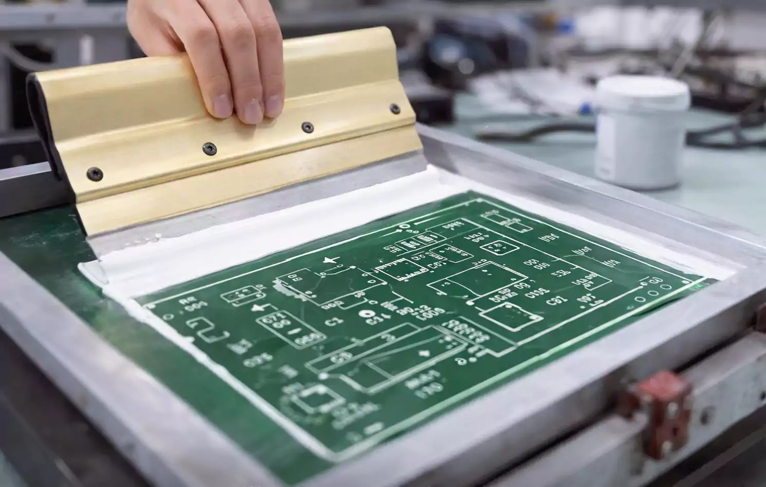
Traditionally, Silkscreen PCB was applied by screen printing—pushing epoxy-based ink through a fine-mesh stencil onto the board.
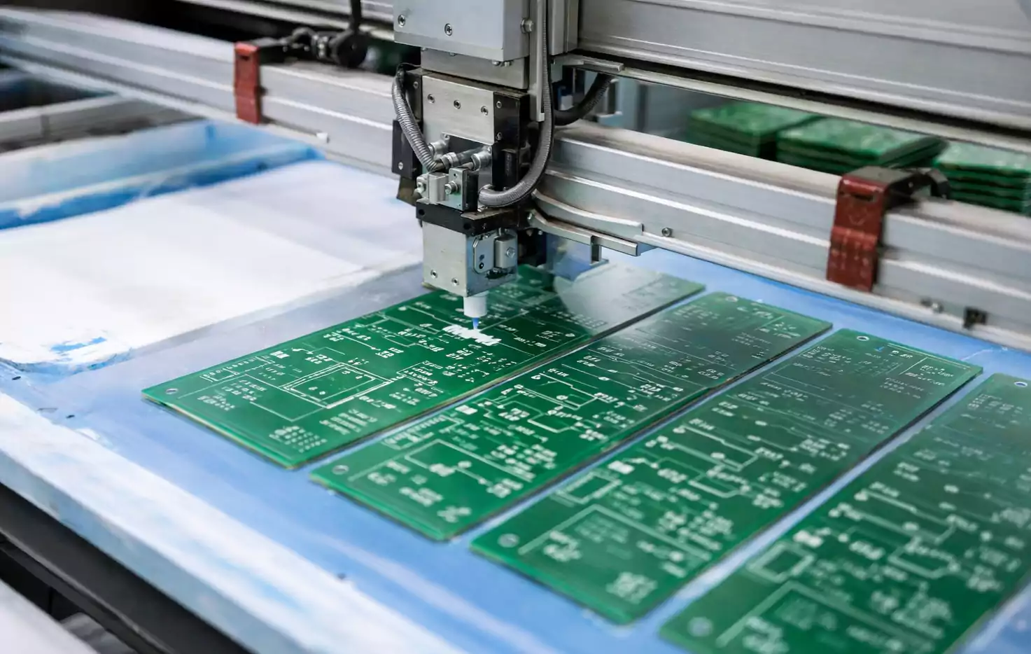
While still common for low-volume work, many fabricators now use liquid photo-imageable (LPI) or direct-legend printing (DLP) systems, including inkjet methods.
| Screen printing | Ink pushed through a mesh stencil | Standard FR-4 boards | Inexpensive, durable | Limited precision |
| LPI (photo-imageable) | Cured by UV light through a film | High-density designs | Sharp edges, consistent | Higher cost |
| Digital inkjet / DLP | UV-curable ink printed directly | Prototyping, branding | Multicolor possible, no tooling | Slightly lower opacity |
Some advanced suppliers even offer multicolor or full-graphic silkscreen, allowing logos, gradients, or educational graphics on development boards. Keep in mind, though, that photographic detail may slightly affect registration tolerance.
What to Include on the Silkscreen
A functional silkscreen does more than just label components. It should communicate essential visual cues to assembly and test technicians.
Common items include:
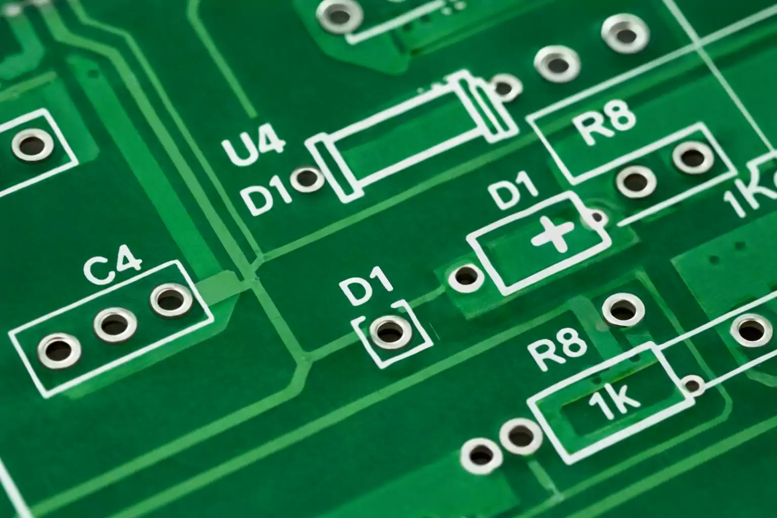
- Reference designators (R1, C5, U7, etc.)
- Component outlines and polarity indicators.
- Pin-1 or orientation markers
- Test points and probe labels
- Mounting holes or keep-out markings
- Revision codes, part numbers, or manufacturer logos
- Safety icons (high voltage, ESD, etc.)
For polarized parts—diodes, electrolytic capacitors, connectors—always ensure Pin 1 or polarity marks are obvious and match the schematic symbol.
Minimum Text Height, Line Width, and Spacing
Silkscreen is only effective if it remains readable after fabrication and soldering.
Each manufacturer has its own process limits, but here’s a consolidated reference range from leading PCB fabs:
| Text height | ≥ 1.0 mm (≈ 40 mil) | 0.8 mm (≈ 32 mil) | 0.6 mm (≈ 25 mil) |
| Line width / stroke | ≥ 0.15 mm (≈ 6 mil) | 0.10 mm (≈ 4 mil) | 0.08 mm (≈ 3 mil) |
| Character spacing | ≥ 0.15 mm | 0.10 mm | — |
Maintaining these values ensures both automated optical inspection (AOI) systems and human assemblers can easily identify components. Overly fine silkscreen text may appear fuzzy or disappear entirely after solder mask and reflow.
Keep the Silkscreen PCB Clear of Pads and Copper
One of the most common fabrication errors is placing text or outlines too close to pads.
During manufacturing, any overlapping ink will be automatically clipped to prevent solderability issues. This can distort or delete part of your markings.
Typical clearance rules (check with your fab’s DFM guidelines):
- Silkscreen to solder mask opening: ≥ 4–8 mil
- Silkscreen to exposed copper pad: ≥ 6 mil
- Silkscreen to board edge or routed slot: ≥ 8–10 mil.
Bad practices to avoid:
- Text crossing open solder mask areas (may burn or flake during reflow).
- Overlapping reference designators with component pads.
- Printing too close to panel break-outs or tooling holes.
A good workflow is to run a DRC (design rule check) in your CAD software, specifically for silkscreen clearance, before generating Gerbers.
QR Codes, Barcodes, and Serialized PCB Labels
Modern electronics manufacturing relies heavily on traceability.
Adding a QR code or a 2D data matrix directly to the silkscreen layer enables automated tracking throughout assembly and testing.
Silkscreen QR vs. Adhesive Labels
| Silkscreen QR code | Permanent, no extra material cost | Larger area needed, limited resolution |
| Laser-engraved code | High contrast, durable | Requires specific substrate and equipment |
| Polyimide label (heat-resistant) | Excellent for reflow and cleaning | Slight extra cost, manual placement |
Size and Placement
- Minimum practical printed QR size: 8–10 mm square for silkscreen; 5 mm possible for laser marks.
- Keep at least 2 mm of clear space around the code.
- Avoid glossy or uneven surfaces that can reflect scanner light.
- Place the code where it remains visible after assembly and conformal coating.
Clarifying “PCB Labels”
Be aware that the term PCB labels can also refer to hazard labels for polychlorinated biphenyls (the chemical compound).
In this context, however, we are referring strictly to electronic PCB labeling for manufacturing traceability.
Fiducial Marks and Silkscreen Coordination
Fiducials are small circular copper pads used by pick-and-place machines for vision alignment.
Good placement and clear visibility are essential for precise component mounting—especially with fine-pitch packages or BGAs.
Best Practices
- Use at least 3 global fiducials, arranged non-collinearly on the PCB, for overall alignment.
- Add local fiducials near dense or high-precision components if required.
- Typical copper diameter: 1–3 mm with a clear solder mask opening and no silkscreen on top.
- Maintain at least 3–5 mm clearance around each fiducial to ensure the camera can detect it cleanly.
Silkscreen Interaction
Ensure no text, lines, or QR codes overlap or crowd around fiducial clearances.
Even small artifacts can confuse vision systems or reduce placement accuracy.
Color Choices and Readability
Silkscreen color choices affect readability and AOI quality.
| Green | White | ★★★★★ |
| Black | Yellow or light gray | ★★★★☆ |
| Blue | White | ★★★★☆ |
| Red | White | ★★★★☆ |
| White | Black | ★★★★★ |
If your design uses a white solder mask, avoid white silkscreen—it will be nearly invisible.
For branding or educational boards, multicolor silkscreen can add personality but may require tighter registration and longer lead times.
FAQs About Silkscreen PCB
Can I place silkscreen directly on pads?
No. Any overlap between the silk screen and exposed copper will be automatically removed during production to prevent solderability issues.
Will the silkscreen survive reflow or cleaning?
Yes—modern epoxy or UV-curable inks are rated to withstand lead-free reflow temperatures and typical cleaning solvents.
Can I print silkscreen on the bottom side?
Absolutely, but expect a minor cost increase due to the additional process step.
How small can silkscreen text be?
Most fabs recommend keeping text at or above 1.0 mm height and 0.15 mm stroke for guaranteed readability.
Does multicolor silkscreen affect cost or lead time?
Yes, slightly. Multicolor printing usually requires digital inkjet systems and may extend turnaround by 1–2 days, depending on the manufacturer.
Final Thoughts
A well-designed Silkscreen PCB enhances your board’s usability, reliability, and brand identity.
By understanding how text size, placement, and labeling interact with real-world manufacturing, you can produce circuit boards that are not only electrically sound but also visually professional and assembly-friendly.
With the right preparation, your silkscreen layer becomes the final polish that turns a functional board into a product engineers love to work with.