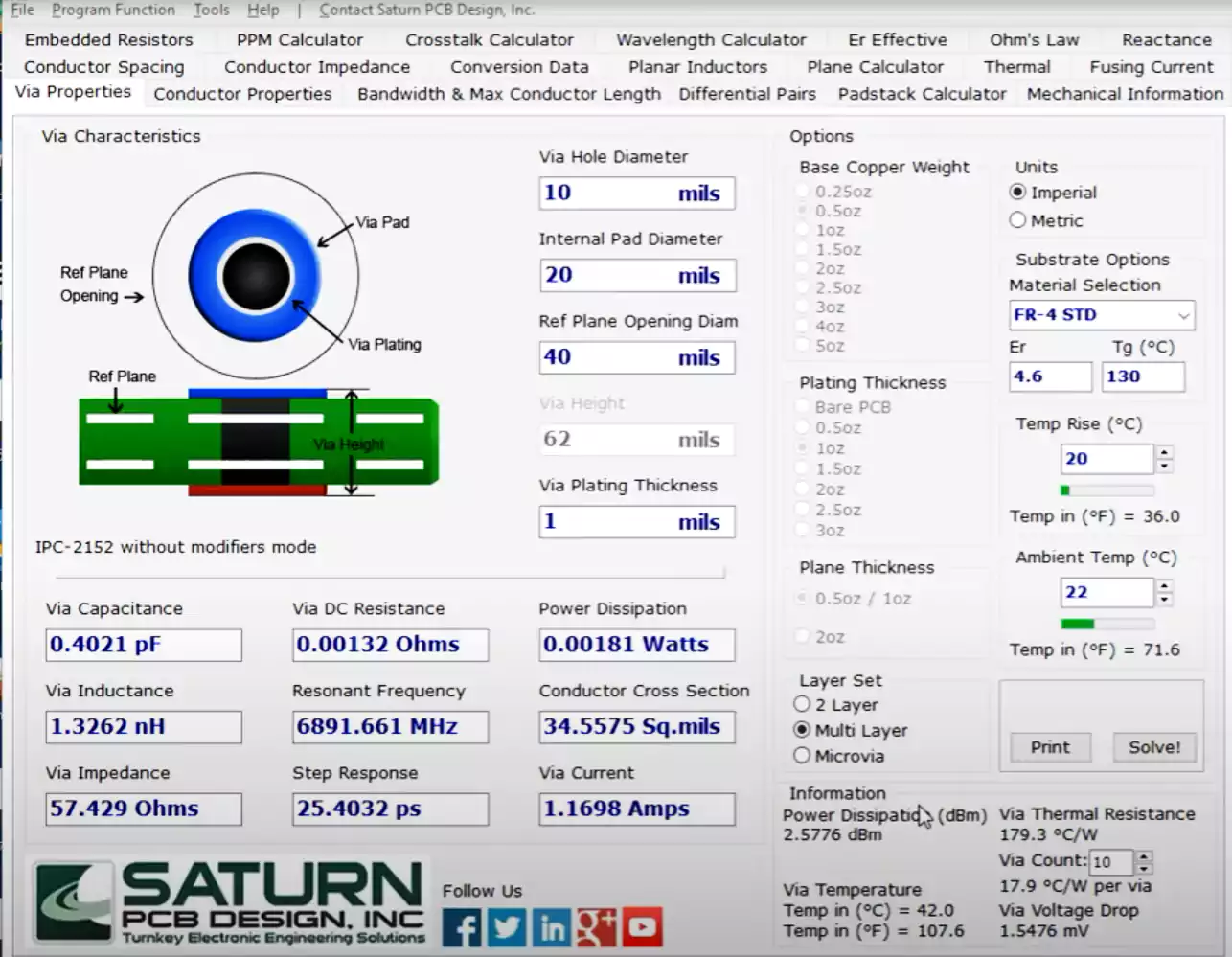
The Saturn PCB Design Toolkit is a trusted free tool for PCB engineers.
You can quickly use this offline utility to find trace width for 10 A, check impedance for a 90 Ω differential pair, or estimate via current.
This guide explains how to use Saturn PCB Toolkit in real design work, how to fix common calculation mistakes, and how to match results with Altium or Polar tools.
Why Engineers Use Saturn PCB Toolkit
When people search for “Saturn PCB” or “Saturn PCB Design Toolkit,” they want a practical calculator.
Typical goals include:
- Calculating controlled impedance (microstrip, stripline, differential pairs).
- Finding trace width vs. current vs. temperature rise according to IPC-2152.
- Checking power loss or voltage drop on a copper trace.
- Understanding why Altium and Saturn give different impedance results.
It features calculators for impedance, copper resistance, via current, and thermal rise in one small Windows app.
Before You Start: The Input Data Matters Most
The quality of your results depends on how you prepare the inputs.
Most errors come from wrong layer thickness, copper plating, or model selection.
a. Use the Real (Pressed) Stackup
Get the pressed dielectric thickness and final copper thickness from your PCB fabricator.
In Saturn, parameters H1 and H2 represent the distance from the signal layer to the top and bottom reference planes after lamination.
Do not enter the raw prepreg thickness.
Wrong H1/H2 is the main reason your impedance values differ from Altium or Polar.
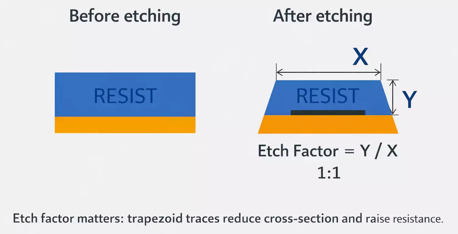
b. Copper Thickness
Make sure the copper value includes base copper plus plating if you are using outer layers.
For differential pairs, both lines should use the same thickness.
If you use 1 oz (≈ 35 µm) base copper with 25 µm plating, the total is ~60 µm.
c. Model Selection
Saturn lets you choose different mathematical models:
| IPC-2152 | Trace width, current, and temperature rise | Based on latest thermal data |
| Wadell / IPC-2141 | Stripline and impedance | Accurate for symmetric cases |
| Default | General use, asymmetric structures | Often closest to field solver results |
Impedance Calculation (Microstrip, Stripline, Differential)
Let’s walk through practical examples you can apply right away.
a. 50 Ω Microstrip (Outer Layer)
- Open Microstrip Impedance Calculator.
- Enter the dielectric height (H), copper thickness (T), dielectric constant (Er), and solder mask if present.
- Choose Target Impedance = 50 Ω, and click Solve for Width.
- Record the line width (W).
Add this data to your controlled impedance note:
Layer = Top, Reference = GND plane, Z₀ = 50 Ω ± 10%, Test @ 1 GHz.
b. 90 Ω Differential Pair
- Select Differential Pair Calculator.
- Input W, spacing (S), H, T, and Er.
- Observe how small spacing reduces impedance — tighter coupling lowers Zdiff.
- Adjust W and S together to hit 90 Ω (for USB 2.0) or 100 Ω (for Ethernet).
Saturn lets you plot how impedance changes when spacing varies — useful for tolerance checks.
c. Asymmetric Stripline (Non-Symmetric Structure)
This is a frequent confusion area in forums.
- Choose Asymmetric Stripline in Saturn.
- Input H1 and H2 carefully — they are different dielectric heights above and below the signal layer.
- Compare results using the Default, Wadell, and IPC-2141 models.
- You’ll often find the Default model gives impedance closer to field-solver or Polar results when H1 ≠ H2.
If the calculated impedance seems twice or half of the expected, double-check your H1/H2 order — it’s a common mistake.
d. Cross-Checking with Altium or Polar
Use the same stackup, copper thickness, and dielectric constants in both tools.
Small differences (1–2%) are normal; large gaps usually mean mismatched definitions or plating not included.
Trace Width, Current, and Temperature Rise
This is the most used section of Saturn — perfect for power and high-current boards.
a. Calculate Trace Width for a Given Current
- Open Trace Width / Current / Temperature Rise.
- Enter current (I), copper thickness, and desired temperature rise (ΔT).
- Click “Solve for Width.”
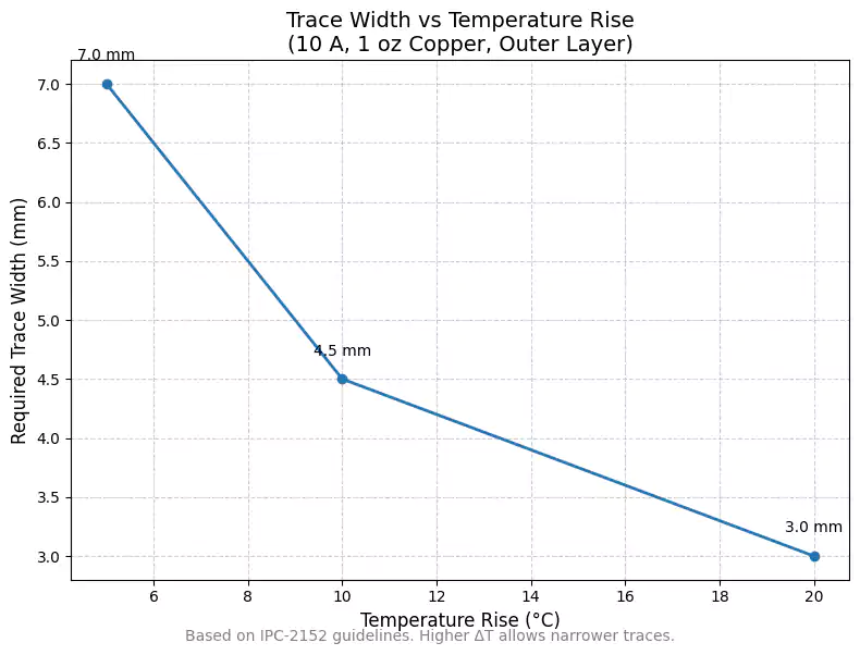
Example: For 10 A current, outer layer, 1 oz copper, ΔT = 10 °C → required width ≈ 4.5 mm (depending on environment).
If you allow a 20 °C rise, the width drops significantly — this shows why ΔT selection is critical.
b. Verify Power Loss and Voltage Drop
Use the Copper Resistance calculator:
- Enter length (L), width (W), and copper thickness (T).
- It gives resistance (R).
- Compute Power = I²R, Voltage Drop = IR.
If Saturn shows identical power or ΔT for different currents, re-check your length and unit settings.
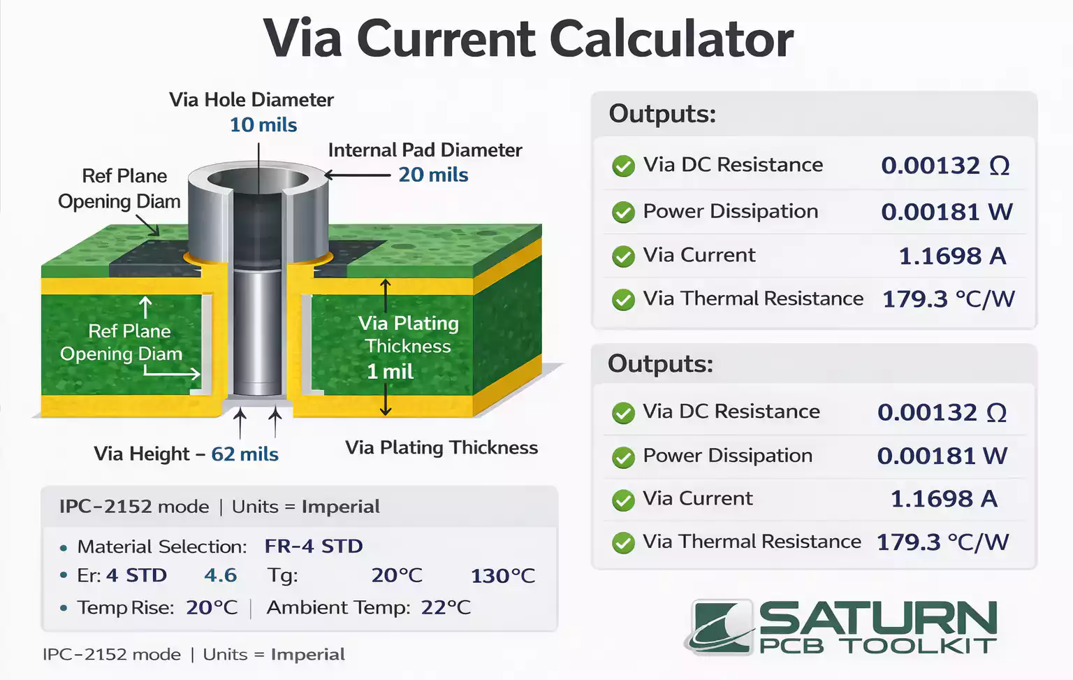
c. Via Current and Parallel Vias
The Via Current module estimates the safe current per via.
To handle higher current, use several vias in parallel.
Remember: two identical vias roughly halve resistance and reduce local heating.
Why Altium and Saturn Show Different Impedance Results
This topic comes up in nearly every engineering forum.
Here’s what usually causes it:
- Layer thickness mismatch – Altium uses prepreg data, Saturn expects pressed data.
- Copper plating is ignored – Altium often uses base copper only.
- Model type – Altium uses IPC-2141 by default; Saturn may default to Wadell or to a custom model.
- Dielectric constant frequency – Er can vary with test frequency.
- Mask layer not considered – outer solder mask lowers impedance a bit.
Correct these mismatches and your tools will agree within 1–2%.
Frequently Asked Questions
Q1. Why is my impedance in Saturn twice the expected value?
Usually, H1 and H2 are reversed, or the model is not suited for asymmetric cases.
Use the “Default” model or double-check your layer order.
Q2. Why do I get the same temperature rise for different currents?
You may have left the length at 0 mm or set the units incorrectly.
Check the resistance and ensure ΔT is calculated in the same environment.
Q3. Which model should I use for high-current traces?
Use IPC-2152, since it reflects updated data for trace heating and cooling.
From Calculation to Fabrication: How to Hand Off Data
Once your Saturn results are ready, include these items in your controlled impedance note for the PCB manufacturer:
- Target impedance (single / differential).
- Tolerance (± 10% typical).
- Reference layer and frequency.
- Final copper thickness and dielectric heights (post-lamination).
- Solder mask presence (yes/no).
Ask your fabricator to verify results using their Polar instrument or in-house solver.
If their numbers differ, review material data together — not every FR-4 behaves the same.
Final Thoughts
The Saturn PCB Toolkit remains a simple but powerful engineering helper.
It bridges the gap between design tools and manufacturing reality — helping you turn math into buildable boards.
By understanding how to set H1/H2 correctly, choosing the right model, and verifying your parameters, you can trust your Saturn results and speak the same language as your PCB fabricator.