


Rigid flex PCB combine the reliability of rigid boards with the flexibility of flex circuits. They are designed to bend, fold, and connect multiple sections while keeping excellent electrical performance. Today, rigid-flex designs are used in everything from cameras and medical devices to satellites and foldable electronics.
This guide explains what rigid-flex PCBs are, how they are built, the key design rules you should follow, and what capabilities Fast Turn PCBs offers for this advanced technology.
What Is a Rigid Flex PCB?
A rigid-flex PCB is a hybrid circuit that combines rigid and flexible layers into a single continuous board. Instead of connecting several rigid boards with cables or connectors, the flexible part acts as an integrated interconnection.
The rigid areas hold and support components, while the flex sections bend and fold to connect them in tight spaces. This combination saves space, reduces weight, and improves reliability by eliminating solder joints and connectors that could fail under vibration or motion.
Rigid-flex boards are made using the same copper-clad laminates as traditional PCBs, but they also include polyimide flexible layers. These layers can bend repeatedly without breaking, allowing the board to fit in compact or movable assemblies.
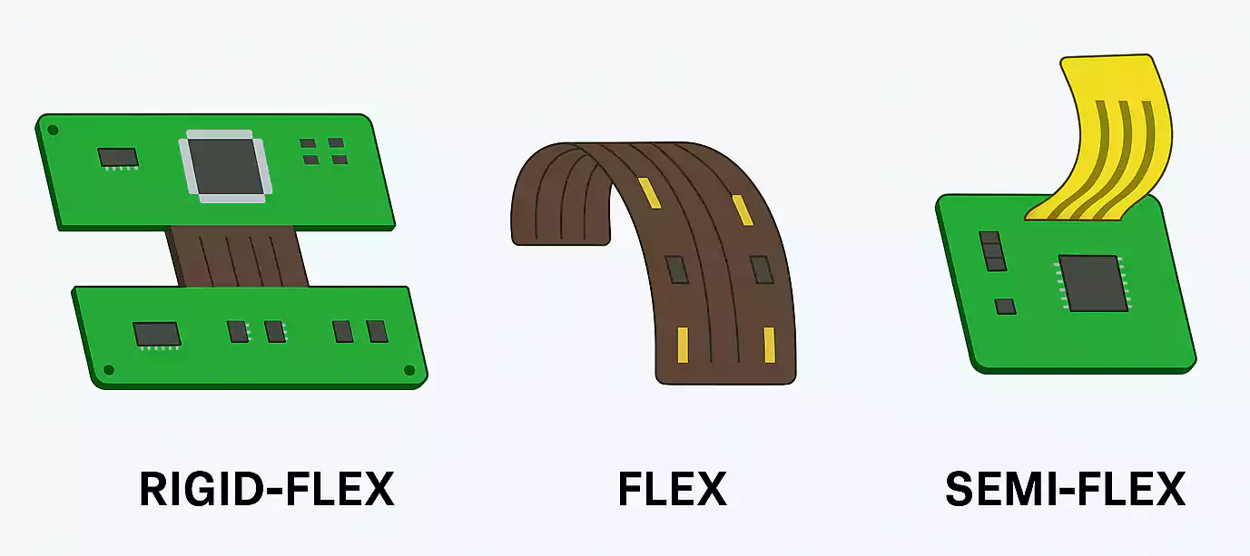
Rigid Flex vs. Flex vs. Semi-Flex
| Rigid-Flex | Rigid FR-4 sections with internal or external flex layers | Up to millions (depending on design) | 0.2–0.8 mm (flex area) | Cameras, medical, aerospace |
| Flex | All-flexible polyimide layers | Continuous bending | 0.1–0.3 mm | Wearables, sensors |
| Semi-Flex | Thin FR-4, locally milled or slotted | Limited (1–5 folds) | 0.2–0.6 mm | Static installations |
Semi-flex PCBs are lower-cost solutions for simple one-time bends, while full rigid-flex boards are best when you need dynamic or repeated movement.
Materials and Typical Stackups
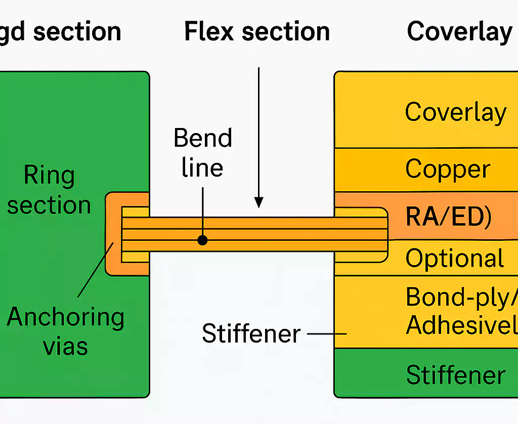
Rigid-flex boards use both flexible and rigid materials in the same stack. The most common flexible substrate is polyimide (PI), chosen for its excellent thermal stability and bend endurance.
Copper foil can be rolled-annealed (RA) or electrodeposited (ED). RA copper is smoother and better for bending, while ED copper is used in rigid zones.
Adhesive systems can be glue-based (bond-ply) or adhesiveless constructions for tighter bend radii and higher reliability. The top of the flex layers is protected by coverlay film, which replaces the solder mask and allows the copper to flex safely.
Stiffeners—made of FR-4, polyimide, or stainless steel—are often added under components or connectors to strengthen flexible areas.
A typical rigid-flex stackup may include four to eight layers, with the flexible layers in the middle and extending into the bend area, while the outer rigid sections are built with FR-4. Keeping the stack symmetrical helps control warpage during lamination.
Rigid Flex PCB Design Rules
Designing rigid-flex PCBs requires early coordination between design and manufacturing. Once the stackup and bend areas are defined, changes become costly. Here are the most important guidelines:
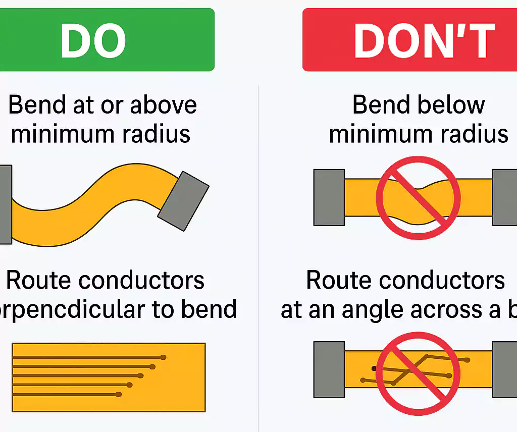
1. Bend Radius
The minimum bend radius depends on the total thickness and the number of layers in the flex region.
- For static bends (folded once during assembly), use at least 10× the flex thickness.
- For dynamic bends (repeated motion), start from 100× the thickness for long life.
Keeping traces in the neutral axis of the bend and minimising overall flex thickness extends fatigue life.
2. Trace Routing
- Route traces along the bend direction, not across it.
- Avoid 90° angles or sharp corners—use smooth curved traces instead.
- Keep an equal copper balance on both sides to prevent curling.
- Use teardrop pads and tapered transitions to reduce stress at vias and pads.
- Avoid large copper pours over the bend area; use hatched patterns if shielding is needed.
3. Vias and Transitions
- Do not place vias inside active bend areas.
- During the rigid-to-flex transition, use “anchoring vias” or via fences to distribute stress and secure the copper layers.
- For multilayer designs, keep the flex region thin and use staggered or blind vias as needed.
4. Coverlay and Solder Mask
Use coverlay openings precisely over pads and fingers; make sure the openings are slightly larger than the copper features. For ZIF connectors, control the exposed copper length and plating thickness.
When designing controlled-impedance traces in the flex area, consider the thinner dielectric and polyimide's different permittivity.
How Rigid Flex PCBs Are Manufactured
The production of rigid-flex PCBs involves more complex steps than standard boards. Each section is processed separately before final lamination. The typical workflow includes:
- Inner Layer Imaging & Etching – Flexible and rigid sub-layers are imaged and etched individually.
- Lamination – Multiple stages of lamination join flexible and rigid materials. Bond-ply or adhesiveless laminates ensure precise alignment.
- Drilling & Plating – Holes are drilled and plated to connect layers. Laser microvias may be added in HDI-style designs.
- Outer Layer Patterning – Rigid sections are etched to form final copper traces.
- Coverlay & Stiffener Lamination – Flexible areas receive protective coverlay films and optional stiffeners.
- Surface Finishing – ENIG, HASL-LF, OSP, or ENEPIG finishes are applied depending on assembly needs.
- Routing & Testing – Laser cutting defines the outline, followed by electrical testing, AOI, and final inspection.
Each lamination cycle must precisely align rigid and flexible layers. Any mis-registration can cause cracks or delamination, so manufacturers use special tooling and vacuum lamination presses.

Fast Turn PCB Capabilities
Fast Turn PCBs provides full rigid-flex manufacturing from prototyping to mass production.
Our capabilities include:
- Layer count: up to 26 layers
- Minimum trace/space: 0.065 mm / 0.065 mm
- Minimum hole/pad: 0.10 mm / 0.35 mm
- Finished copper thickness: flex area 0.5–2 oz, rigid area 1–4 oz
- Board thickness range: 0.25–6.0 mm
- Maximum panel size: 620 × 500 mm
- Surface finishes: ENIG, HASL-LF, OSP, Immersion Silver, Immersion Tin, Hard Gold, ENEPIG
- Hole tolerance: ± 0.05 mm
- Typical lead time: 7–20 days, with expedited service available
With engineering review and DFM feedback at every stage, we help customers shorten development cycles and avoid costly redesigns.
Assembly and Reliability Tips
Component placement and soldering require extra care on rigid-flex PCBs.
- Mount heavy or heat-sensitive components on rigid areas.
- If components must be on a flex zone, use stiffeners under them for support.
- During reflow, the flexible parts should be clamped or supported to prevent sagging.
- Avoid repeated bending after assembly unless the design specifically allows dynamic flexing.
- During shipping or handling, mark the bend direction clearly to prevent damage.
Pros, Cons, and Best-Fit Applications
Advantages
- Fewer connectors and solder joints → higher reliability
- Reduced weight and thickness for compact devices
- Ability to fit 3D enclosures and complex shapes
- Better performance in vibration or thermal stress environments
Challenges
- Higher initial cost and longer manufacturing lead time
- Tighter design rules for bend areas and transitions
- More communication is required between the design and fabrication teams.
Typical Applications
Rigid-flex PCBs are widely used in:
- Cameras and mobile modules
- Wearable electronics
- Medical equipment and implants
- Aerospace and military systems
- Automotive radar and control units
- Industrial sensors and control boards
Wherever space, reliability, and vibration resistance matter, rigid-flex designs are often the best choice.
Common Pitfalls to Avoid
Even experienced designers can run into issues if rigid-flex details are overlooked:
- Placing vias or BGA fan-outs directly in bend zones
- Forgetting to mark bend lines and bend radius on drawings
- Coverlay openings not matching pad sizes
- Continuous solid copper planes crossing bend lines, which can crack over time
Avoiding these mistakes early can save expensive respins and delays later.
Mini-Guide: How to Bond Flex to Rigid
The transition between flex and rigid sections is the most critical area of the design.
Manufacturers typically use step-stack structures, in which the rigid layers gradually thin near the flex region. Anchoring vias help lock copper layers and prevent delamination.
Adding relief slots or diamond-shaped cutouts at the transition can spread mechanical stress. For best results, use adhesiveless polyimide laminates for tight-bend designs—they offer better adhesion and heat resistance than glue-based materials.
FAQs
1. What is a rigid-flex PCB?
A rigid-flex PCB is a circuit board that combines rigid and flexible materials. The rigid parts hold components, while the flexible layers allow the board to bend or fold, reducing the need for connectors and saving space.
2. How are rigid-flex PCBs made?
They are built through multiple lamination steps. Rigid and flexible sub-layers are fabricated separately, aligned, laminated together, drilled, plated, finished, and finally cut to shape before testing.
3. How to bond flex to rigid correctly?
Use step-stack transitions with anchoring vias and relief cutouts. Keep adhesive thickness uniform and select polyimide materials that handle both thermal and mechanical stress.
4. What’s the difference between rigid-flex and semi-flex PCBs?
Rigid-flex boards have true polyimide flex layers and can bend many times. Semi-flex boards are thin FR-4 designs that bend only a few times during assembly.
5. What capabilities does Fast Turn PCBs offer?
We can produce up to 26 layers, with 0.065 mm line/space, 0.10 mm holes, and flexible copper from 0.5–2 oz. Typical turnaround is 7–20 days, and expedited builds are available.
Conclusion
Rigid-flex PCB deliver unmatched design freedom, reliability, and space savings for modern electronic products. By understanding their materials, stackups, and design rules, engineers can unlock new possibilities for 3D layouts and high-density interconnections.
Fast Turn PCBs provides complete rigid-flex manufacturing—from prototype to production—with advanced equipment, 24/7 engineering support, and quick delivery.
Upload your Gerber or ODB++ files today and get a professional DFM review before your next build.
