


In RF PCB Design, one of the most overlooked yet critical truths is this:
Not all PCBs are designed the same way.
A Printed Circuit Board (PCB) or PWBI is far from a one-size-fits-all platform. Depending on its end application, the board’s materials, design goals, routing rules, and manufacturing methods can differ dramatically. Treating all PCBs with the same design logic often leads to instability, excessive debugging, or even total product failure.
From an engineering perspective, PCBs generally fall into two broad categories:
- Analog, RF, and Microwave PCBs – used in stereo systems, RF transmitters and receivers, power supplies, automatic control systems, and microwave devices.
- Digital PCBs – found in computers, signal processors, gaming consoles, printers, and other complex digital systems.
The difference between them is not simply about frequency — it’s about design philosophy.
Let’s take a closer look at what makes RF PCB Design and microwave PCB design so unique.
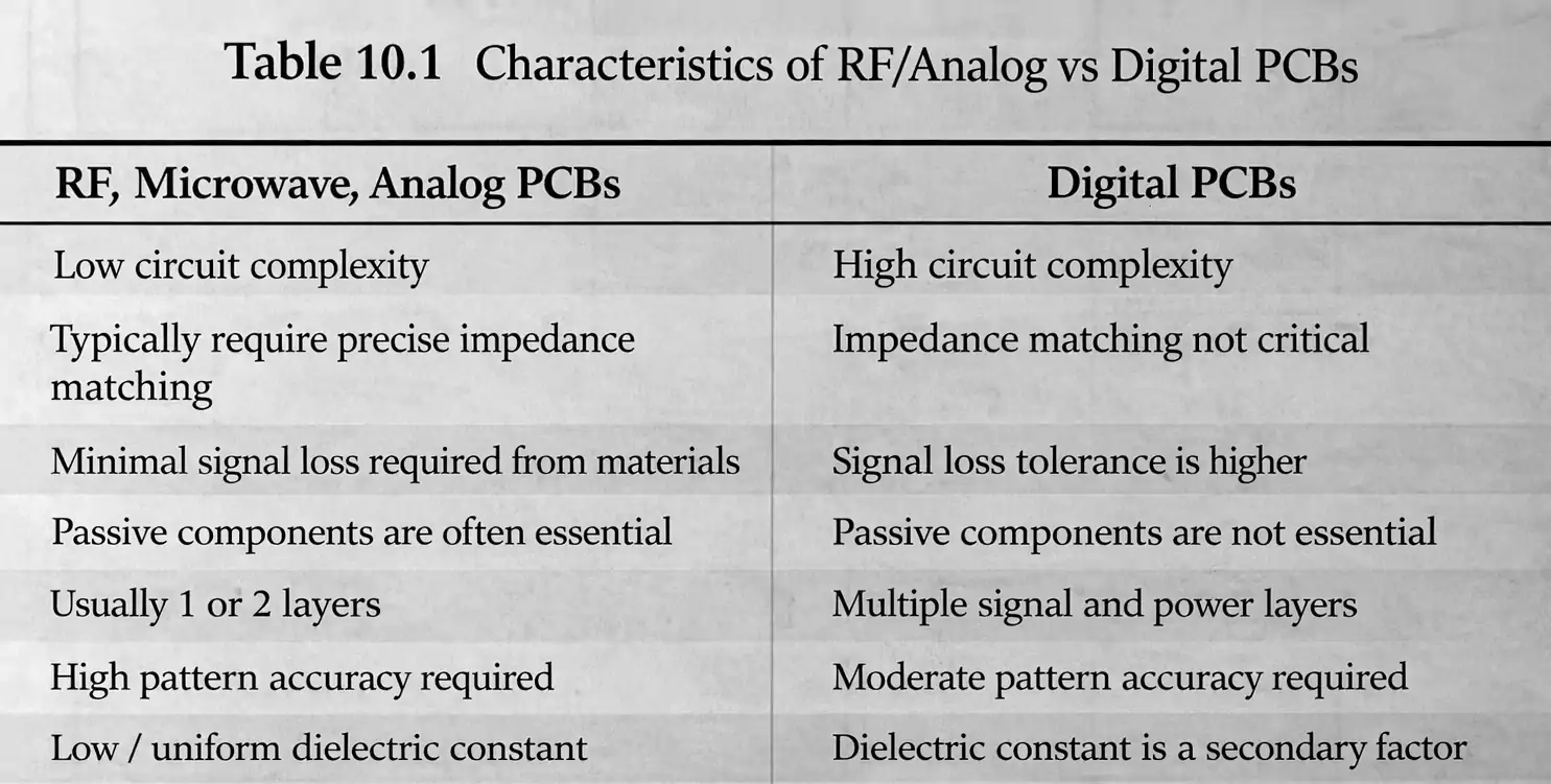
Core Design Characteristics of Analog, RF, and Microwave PCBs
Compared with digital PCBs, analog and RF PCBs are closer to electromagnetic structure design than pure electrical interconnection.
At first glance, these boards look simple: most components have only 2 to 4 leads and consist mainly of resistors, capacitors, transistors, inductors, and transformers. The schematics appear far less complex than those of digital systems.
But the real challenge lies elsewhere — in RF and microwave frequencies, the PCB itself becomes an active part of the circuit.
1. Lower Circuit Complexity, but Physical Effects Dominate
In RF PCB design, even a minor geometric feature can affect signal behavior.
The design is not about how many components you place, but how the board’s physical structure interacts with electromagnetic energy.
Every trace, pad, and via introduces parasitic effects that can make or break circuit performance.
2. Traces, Pads, and Vias Are Part of the Circuit
In low-frequency or digital circuits, traces are treated as ideal conductors. But in an RF PCB, this assumption quickly breaks down.
- A trace behaves as a distributed inductor and capacitor.
- A pad contributes localized capacitance.
- A via introduces inductance and potential coupling paths.
These parasitic elements are not minor side effects—they actively shape circuit performance.
In some cases, they form the resonant part of an RF amplifier. In others, they degrade the system response.
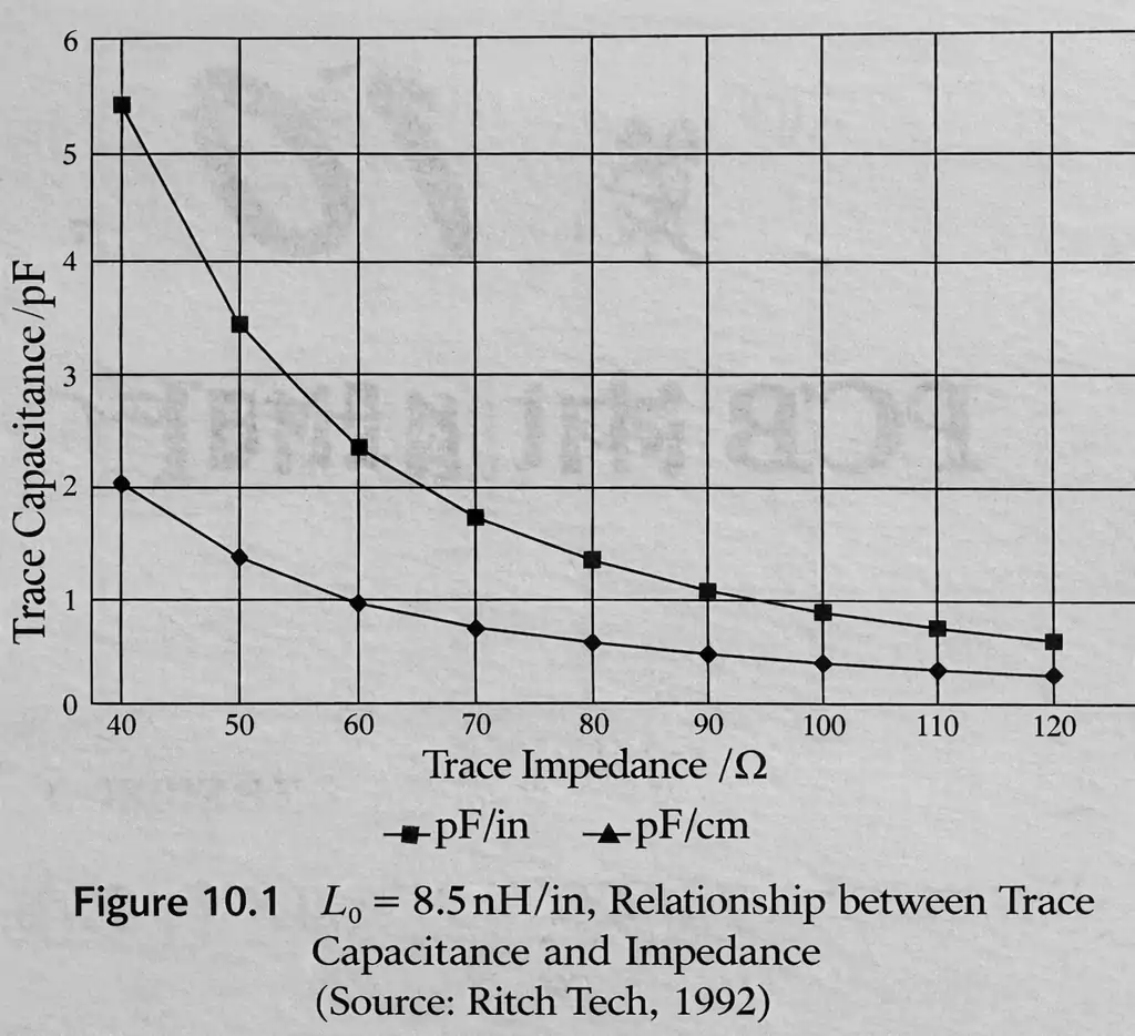
That’s why, in RF PCB design, parameters like trace length, width, bend radius, and impedance must be carefully controlled.
3. Parallel Traces Cause Significant Signal Coupling
When two conductors run in parallel on an RF PCB, they inevitably create electromagnetic coupling.
In a microwave power amplifier, such coupling is intentional—used to form directional couplers or hybrid circuits. But in unintended areas, it becomes a significant source of crosstalk and interference, potentially leading to logic errors or oscillations.
This highlights a key concept in RF and microwave PCB design:
Geometry defines function.
4. Parallel Conductors Can Act as Band-Pass Filters and Introduce Phase Distortion
Specific PCB layouts with multiple parallel conductors can behave like band-pass filters. Ideally, these structures should allow all frequency components to pass simultaneously.
In practice, different frequencies travel at different speeds through the dielectric, arriving at the output at different times. The result is waveform distortion, commonly known as phase distortion.
The culprit? Often, the PCB material itself.
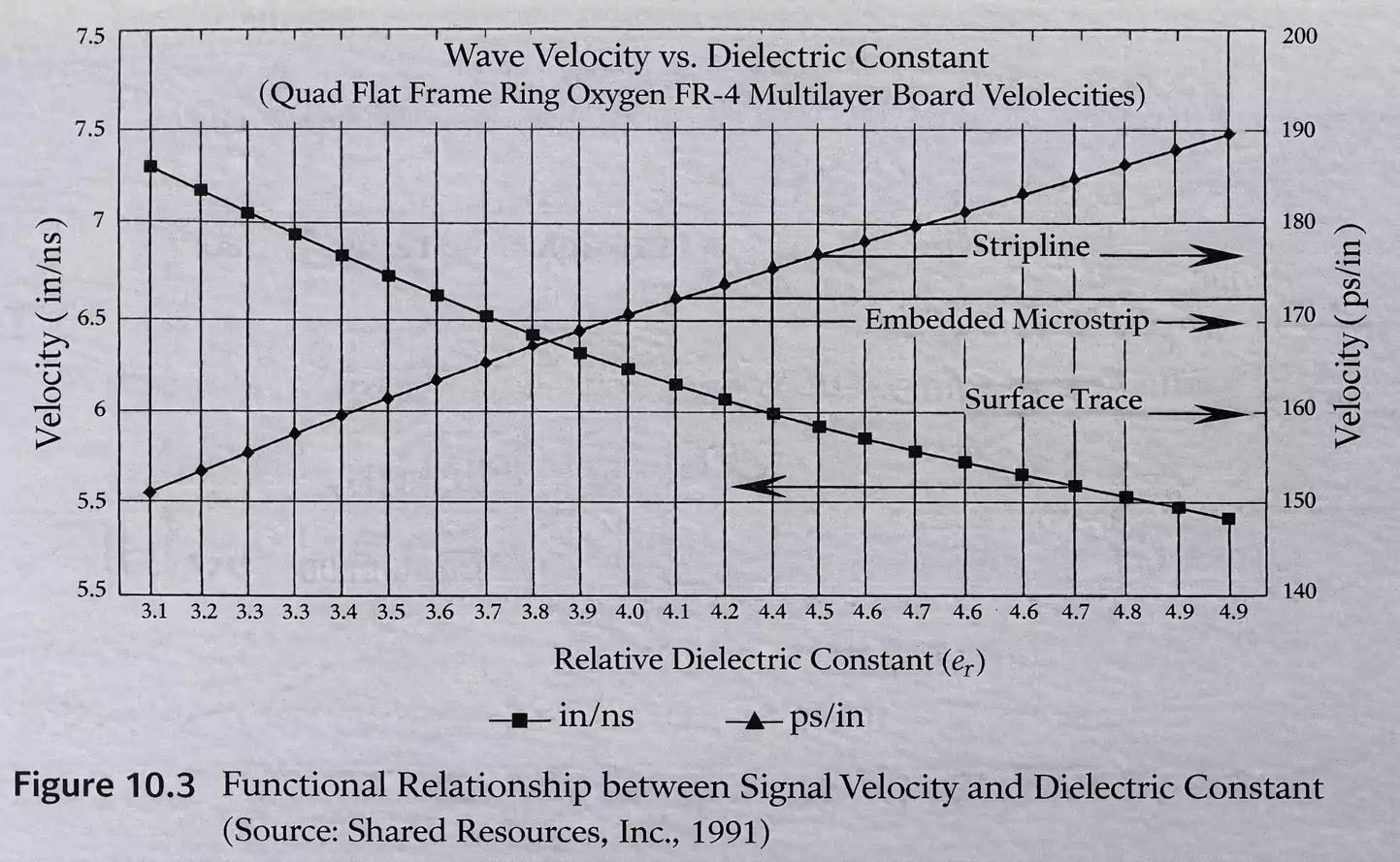
5. Dielectric Constant Variation — The Hidden Killer in RF PCB Design
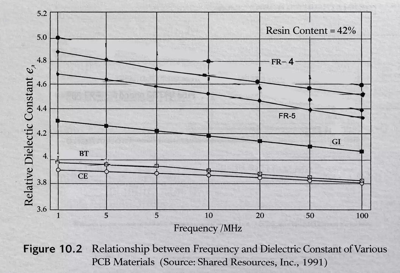
A microwave PCB or RF PCB never operates in a perfect dielectric environment.
Many materials exhibit dielectric constants (Dk) that vary with frequency — some even drop sharply at high frequencies.
Since signal propagation speed is inversely related to the square root of Dk, any inconsistency in dielectric properties leads to unequal propagation speeds:
- High-frequency components arrive earlier.
- Low-frequency components lag.
- The output waveform stretches or distorts.
In RF and microwave applications, using a material with non-uniform dielectric behavior inevitably introduces phase distortion and compromises signal integrity.
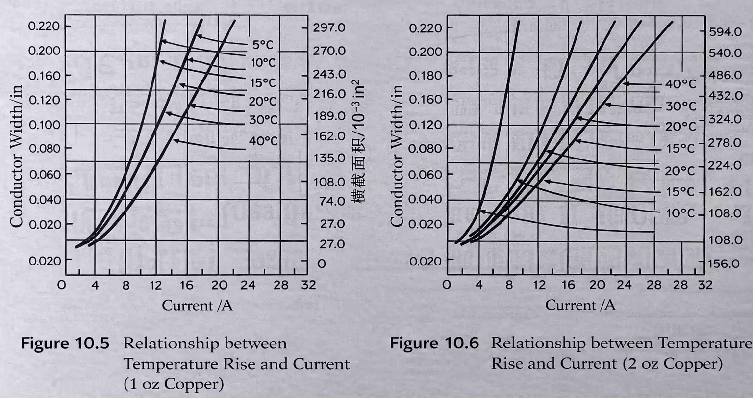
6. Power Conductors Are Not Just “Power Lines.”
Even without noticeable heating or voltage drop, PCB conductors in power circuits can carry several amps of current.
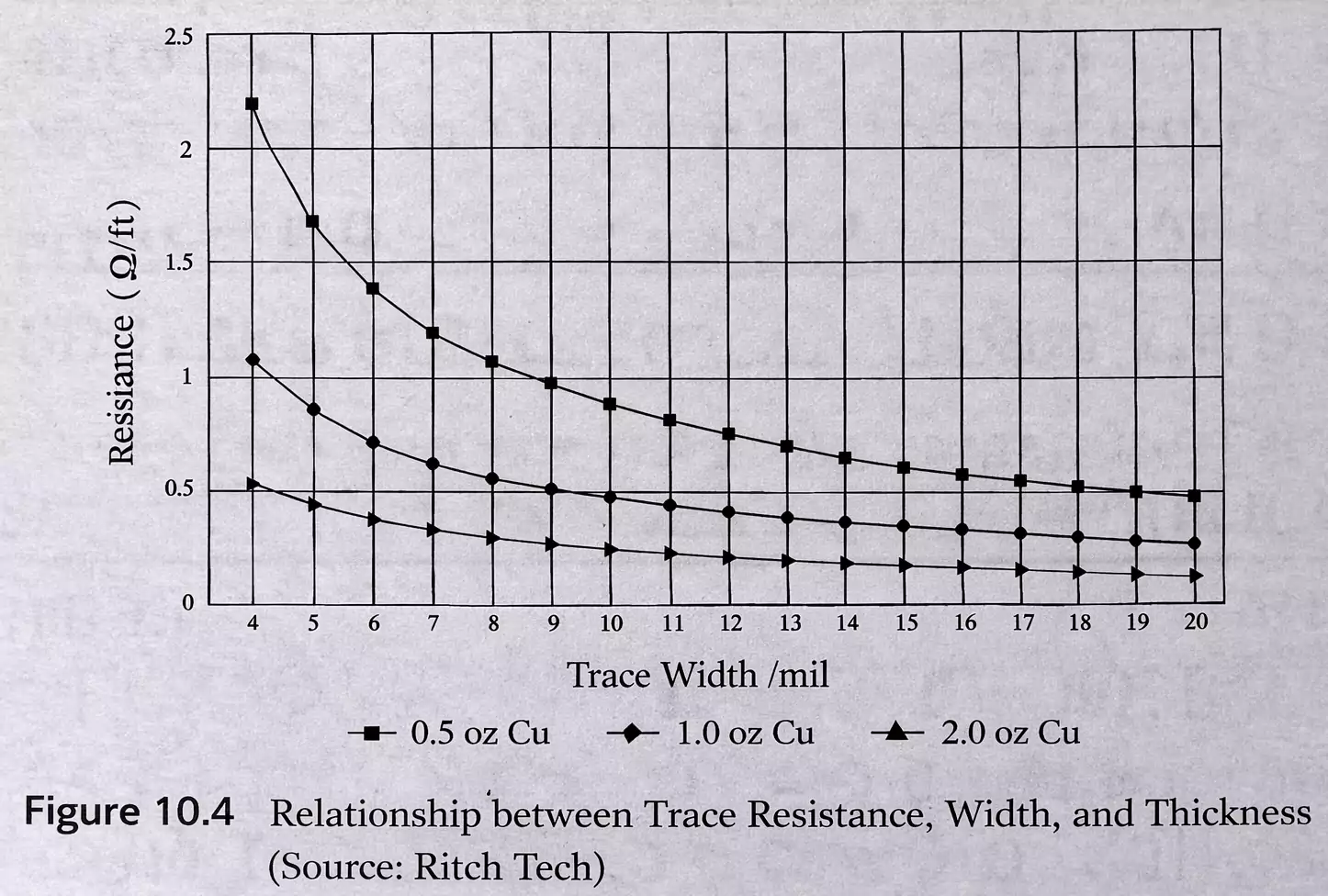
- Their resistance can be used intentionally for current sensing.
- Inadequate copper thickness or trace width can cause excessive voltage drop.
- Heat rise further reduces performance and reliability.
Therefore, in analog and RF PCB design, power routing is a performance parameter rather than just a mechanical concern.
7. Consumer Electronics PCBs: Optimized for Cost, Not Performance
Consumer electronics PCBs often resemble analog or RF boards in structure, yet their design goals are entirely different.
Here, performance requirements are modest, and cost reduction dominates every decision. Common strategies include:
- Keeping all routing on a single layer whenever possible
- Punching holes instead of drilling or plating
- Avoiding expensive metallization processes
- Using paper-based resin substrates to minimize cost
In this context, performance takes a back seat to manufacturability and cost efficiency.
RF PCB Design FAQs
What is RF PCB design?
RF PCB design is the process of creating printed circuit boards for high-frequency applications such as radio, wireless, or microwave systems. It focuses on impedance control, material selection, and electromagnetic behavior to maintain signal integrity.
How does RF PCB design differ from digital PCB design?
In digital PCBs, traces mainly act as conductors. In RF and microwave PCBs, every trace, pad, and via behaves as part of the circuit—adding inductance, capacitance, and coupling that directly affect performance.
Why is the dielectric constant important?
The dielectric constant determines signal speed through the substrate. If it varies with frequency, phase distortion occurs, causing timing and integrity issues in RF circuits.
What materials are used for RF and microwave PCBs?
High-frequency designs typically use Rogers, Taconic, or PTFE-based laminates with stable dielectric properties. FR-4 is suitable only for low-frequency or cost-sensitive applications.
What are key layout considerations in RF PCB design?
Controlled impedance routing
Short and direct signal paths
Consistent ground planes
Proper spacing to limit coupling
Precise geometry and material consistency are essential for predictable performance.
What defines a successful RF PCB design?
A successful RF PCB design achieves low loss, stable impedance, and minimal phase distortion across its operating frequency range by balancing material choice, structure, and layout precision.
Conclusion
Ultimately, successful RF PCB design and microwave PCB design depend less on circuit complexity and more on the physical properties of materials, conductor geometry, and spatial relationships between traces.
That’s why RF PCB layout remains a highly specialized craft. It relies heavily on engineering experience, manual routing, and an understanding of electromagnetic behavior, rather than full automation.
To build reliable, high-performance RF and microwave circuits, designers must select appropriate substrate materials, control all geometric variables, and use design tools capable of accurately modeling electromagnetic effects.
In the world of RF PCB design, precision is not optional — it’s everything.
