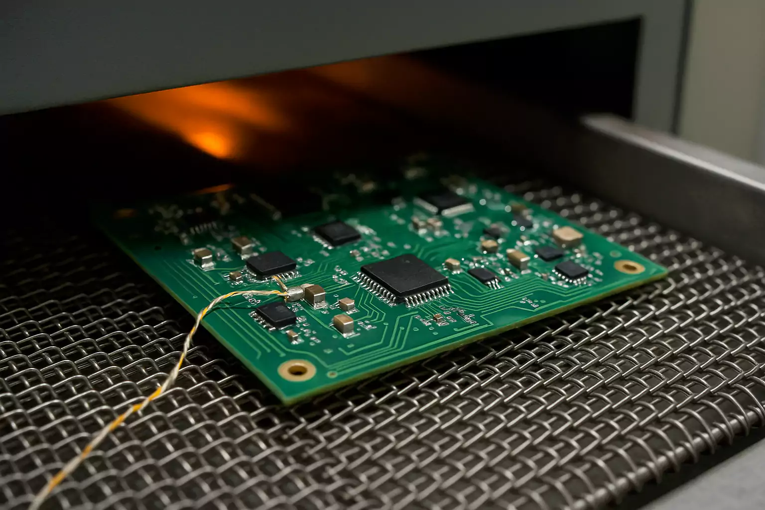
What is Reflow Soldering?
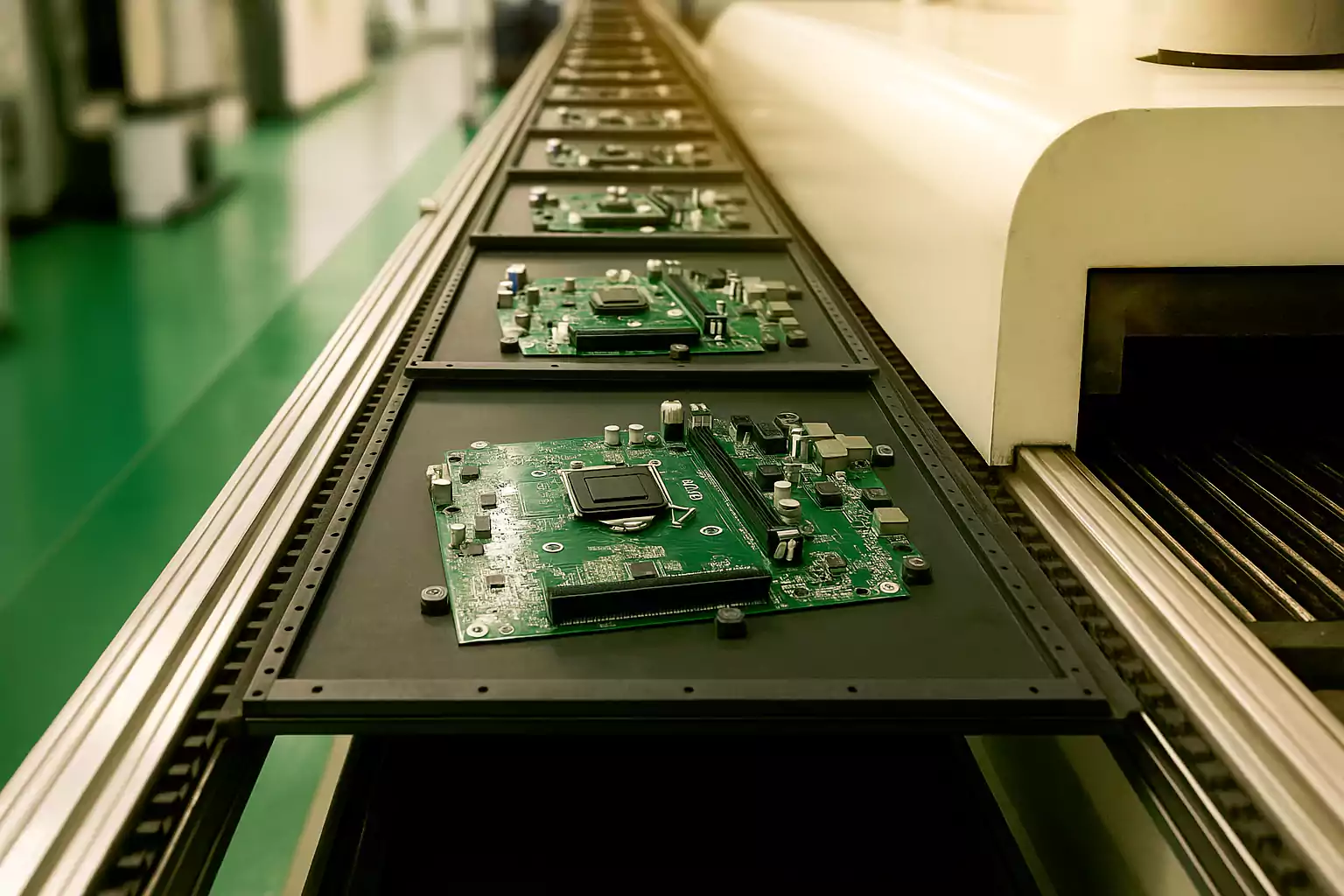
Reflow soldering is the most widely used method for permanently attaching surface-mount components to a printed circuit board (PCB). In this process, a layer of solder paste—made of powdered solder alloy and flux—is first deposited onto PCB pads using a stencil. Components are then carefully placed on top of the paste. The entire assembly is passed through a controlled heating system, usually a multi-zone reflow oven, where the solder paste melts, flows, and solidifies to create reliable electrical and mechanical connections.
The primary purpose of reflow soldering is to ensure strong, consistent joints between fine-pitch surface-mount devices (SMDs) and the PCB, while minimizing stress on sensitive components. Unlike manual soldering or wave soldering, reflow provides precise temperature control across multiple heating zones, making it suitable for high-density boards and modern electronics manufacturing.
In surface-mount technology (SMT), reflow soldering plays a critical role by:
- Supporting miniaturization: It allows the use of very small and closely spaced components.
- Ensuring repeatability: Controlled temperature profiles guarantee consistent joint quality in mass production.
- Reducing defects: Optimized profiles help prevent common issues such as tombstoning, cold joints, and voids.
How it began
Reflow soldering emerged as the electronics industry transitioned from manual soldering to automated surface-mount technology (SMT) in the late 20th century. Early SMT production relied on leaded solder alloys, primarily tin-lead (SnPb), which offered a relatively low melting point (183 °C) and reliable wetting properties. These characteristics made it easier to create consistent solder joints while protecting components from excessive thermal stress.
However, growing environmental and health concerns about lead usage drove regulatory changes worldwide. The Restriction of Hazardous Substances (RoHS) Directive, introduced in the early 2000s, accelerated the shift toward lead-free solder pastes such as SAC alloys (tin-silver-copper). Lead-free solders require higher peak reflow temperatures—typically 235–250 °C compared to 205–220 °C for leaded solder—making temperature profile optimization more critical than ever.
At the same time, organizations like JEDEC and IPC published standards that define reflow temperature limits, component classification, and process guidelines. These industry standards provide manufacturers with a framework to ensure product reliability while adapting to new solder chemistries.
Today, reflow soldering is the dominant method for SMT assembly, used across industries from consumer electronics to aerospace. Its evolution from leaded to lead-free processes highlights the importance of precisely controlled thermal profiles—not only to comply with regulations, but also to maintain solder joint integrity and long-term product performance.
How Does Reflow Soldering Work?
Reflow soldering forms the electrical and mechanical connections between surface-mount components and PCB pads using pre-applied solder paste. The process involves passing the PCB through a controlled heating cycle inside a reflow oven. The temperature profile must be carefully tuned to ensure complete solder reflow while preventing defects.
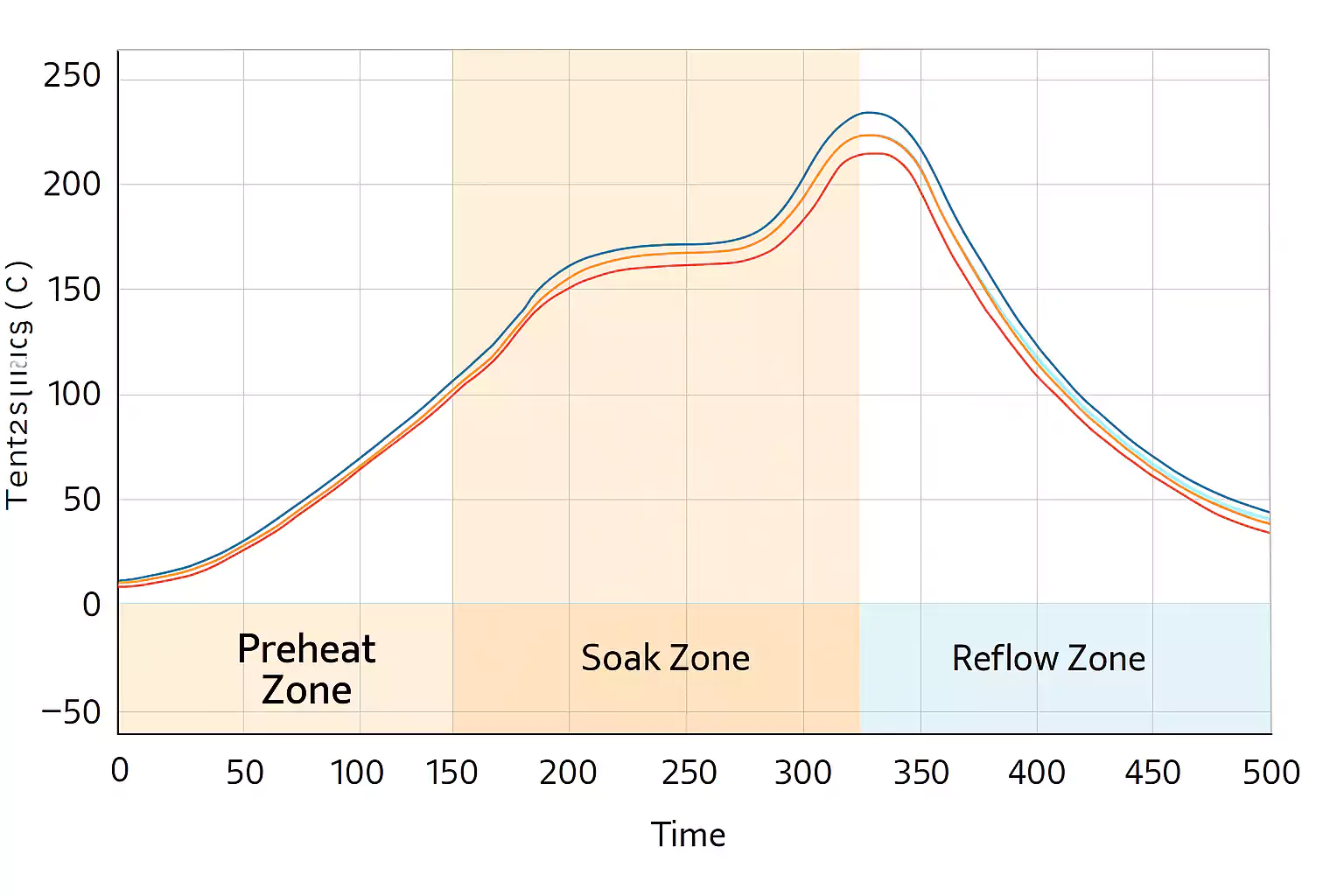
Four Stages of the Reflow Profile
1. Preheat
The board temperature ramps up gradually—typically at 1.5–3 °C/sec—to reduce thermal shock and begin flux activation. This stage evaporates solvents in the solder paste and brings the entire assembly to a uniform temperature.
2. Soak
The soak zone allows temperature stabilization across components. It typically holds the PCB between 150–180 °C (for leaded) or 170–190 °C (for lead-free) for 60–120 seconds. Soak also completes flux activation and prepares the solder for reflow.
3. Reflow (Peak)
The temperature exceeds the solder alloy’s melting point by 20–30 °C to form proper metallurgical bonds. For SnPb solder, peak temperatures range from 205–220 °C. For SAC alloys (lead-free), 235–250 °C is typical. The time above liquidus (TAL) should be maintained between 30–60 seconds to ensure full reflow without overheating components or promoting brittle intermetallic growth.
4. Cooling
Rapid, controlled cooling—at 3–6 °C/sec—is critical to forming strong solder joints. A proper cooling rate prevents warping, minimizes residual stress, and controls solder grain structure.
Profile Types
- Ramp-Soak-Spike (RSS): Incorporates a soak zone to equalize heat distribution. Ideal for densely populated boards or mixed components.
- Ramp-to-Spike (RTS): Eliminates the soak zone for faster throughput. Best suited for simpler assemblies.
Oven Operation
Modern reflow ovens use multiple heating zones with programmable temperatures. Conveyor speed and zone control are adjusted to match the required profile. Proper profiling is essential and should be validated using thermocouples and profiling tools.
Reflow Soldering Temperature Profile Considerations
Establishing the correct temperature profile is the most critical factor in achieving high-quality solder joints in SMT assembly. A well-optimized profile minimizes soldering defects such as tombstoning, cold joints, voids, and component damage. The following considerations guide process engineers and SMT operators through each stage of profile design.
Solder Paste Type (Lead vs. Lead-Free)
The solder paste formulation determines the melting point and target reflow conditions.
- Lead-based solder (Sn63/Pb37) melts at ~183 °C, with recommended peak temperatures between 205–220 °C.
- Lead-free solder (SAC305 or similar) melts at ~217–221 °C, requiring higher peak temperatures of 235–250 °C.
Preheat Rate & Soak Duration
The preheat stage gradually raises the PCB temperature to prevent thermal shock and drive off volatiles in the solder paste.
- Typical ramp rate: 1.5–3 °C/s (not exceeding 3 °C/s).
- Target temperature:Leaded: 120–150 °C,Lead-free: 150–180 °C
- Soak duration: Maintain 60–120 seconds in the soak zone (150–180 °C for leaded, 170–190 °C for lead-free).
Peak Temperature & Time Above Liquidus (TAL)
The reflow or peak stage ensures the solder alloy fully melts and wets component leads and pads.
- Peak temperature:Leaded: 205–220 °C,Lead-free: 235–250 °C
- Time Above Liquidus (TAL): Maintain 30–60 seconds above the alloy’s melting point.
Risks:
- Too low → incomplete wetting and cold joints.
- Too high or prolonged → intermetallic compound (IMC) overgrowth, brittle joints, and component overheating.
Cooling Rate
Proper cooling solidifies solder joints and influences microstructure.
- Recommended cooling rate: 3–6 °C/s.
- If too slow → coarse grain growth, reduced joint reliability.
- If too fast → thermal shock, component warpage, or cracked joints.
A controlled cooling phase balances solder strength with mechanical stability.
Board and Component Considerations
When optimizing a reflow soldering profile, it is not enough to rely solely on general temperature ranges. The physical properties of the PCB and the components assembled on it play a critical role in how heat is absorbed, transferred, and dissipated. Engineers must consider these factors to avoid uneven heating, thermal damage, or incomplete solder joints.
PCB Thickness and Thermal Mass
The thickness of the printed circuit board (PCB) directly affects how quickly it responds to heat.
- Thicker boards have higher thermal mass and require longer soak times or slightly higher temperatures to ensure that internal layers and vias reach the correct reflow temperature.
- Thinner boards heat up more quickly but are prone to warpage if the heating and cooling rates are not controlled carefully.
Component Thermal Sensitivity
Different components exhibit varying tolerance to heat.
- Heat-sensitive components such as plastic connectors, LEDs, or crystal oscillators may degrade or shift performance if peak temperatures are too high. In these cases, component-specific maximum reflow ratings (often specified in JEDEC J-STD-020) should be strictly observed.
- Large components (e.g., transformers, shielded inductors) act as heat sinks and may not reflow properly if the profile does not allow enough time above liquidus.
Mixed Component Sizes and Density
Modern SMT assemblies often include a mix of very small passive chips and larger IC packages. This creates challenges in achieving a uniform temperature profile:
- Small passives heat rapidly and are susceptible to tombstoning if temperature gradients are too steep.
- Large BGAs or QFNs require sufficient TAL to ensure complete wetting beneath the package.
- Boards with high component density may experience localized heating differences, making thermal profiling and process window adjustments essential.
Design and Layout Impact
The PCB layout itself influences thermal performance:
- Heavy copper pours or ground planes absorb significant heat, slowing down temperature rise in those regions.
- Uneven component distribution can create hot and cold spots during reflow.
Careful profiling and adjustments to conveyor speed, zone temperature, or airflow can help mitigate these effects.
Common Defects and Prevention
1.Tombstoning
Occurs when small passives lift due to uneven pad heating.
Prevention: Balanced pad design, controlled preheat, and accurate placement.
2.Cold Solder Joints
Result from low peak temperature or insufficient time above liquidus.
Prevention: Maintain 20–30 °C above alloy melting point with 30–60 s TAL.
3.Solder Balling
Caused by excessive paste or rapid heating.
Prevention: Correct stencil design, controlled ramp rate, proper paste handling.
4.Graping
Porous joints from oxidation or prolonged TAL.
Prevention: Use fresh paste, limit TAL, and apply nitrogen atmosphere if available.
5.IMC Brittleness
Excessive heat thickens intermetallic layers.
Prevention: Keep peak temperature within limits and minimize reflow cycles.
6.PCB Warpage
Uneven heating or cooling shifts components.
Prevention: Maintain 3–6 °C/s cooling, use board supports, and design for copper balance.
How to Take a Reflow Soldering Profile
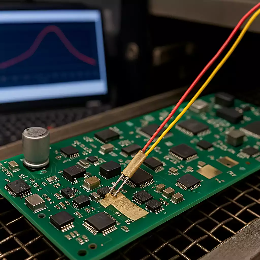
Creating an accurate reflow soldering profile is essential for ensuring process stability, preventing soldering defects, and complying with IPC and JEDEC standards. A temperature profile represents the actual thermal experience of the PCB as it passes through the reflow oven. Below are practical steps and methods to capture and optimize a reflow soldering profile:
Use Thermocouples for Measurement
- Attachment: Place thermocouples on critical points such as the largest thermal mass component, the smallest passive (risk of tombstoning), and the PCB corner or center. Use high-temperature epoxy or Kapton tape for reliable contact.
- Data Collection: Connect the thermocouples to a data logger that travels through the oven with the PCB to capture real-time temperature changes.
Establish a Baseline Profile
- Run the board through the oven with standard settings.
- Record the four phases of the profile (preheat, soak, reflow/peak, cooling).
- Compare the measured values against recommended limits (e.g., preheat slope < 3 °C/s, TAL 30–60 s, peak 235–250 °C for lead-free).
Apply the Process Window Index (PWI)
- Definition: PWI is a statistical measure showing how well the profile fits within the defined process window. A lower PWI indicates a more stable and repeatable process.
- Target: Most manufacturers aim for a PWI below 100%, with < 80% preferred for robust production.
- Benefit: PWI quantifies process margin, helping engineers identify whether adjustments are necessary.
Use Virtual Profiling and DOE Methods
- Virtual Profiling: Modern profiling systems use oven recipes and modeling software to simulate profiles without running multiple trial boards. This reduces downtime and material waste.
- Design of Experiments (DOE): DOE methods help determine the effect of conveyor speed, zone temperature, and airflow on the thermal profile, allowing engineers to find the optimal balance quickly.
Fine-Tune and Verify
- Adjust oven settings (zone temperatures and conveyor speed) iteratively until all parameters meet the target ranges.
- Verify by running additional test boards and ensuring repeatability across production batches.
Conclusion
A well-optimized reflow soldering profile ensures consistent joint quality, minimizes defects, and supports long-term product reliability. By aligning solder type with proper thermal settings across preheat, soak, peak, and cooling stages, engineers can maintain process control in both leaded and lead-free environments.
Effective profiling is not just about meeting temperature targets—it's about enabling a stable, efficient assembly line.