Introduction: What Is Reflow Soldering and Why It Matters
Reflow soldering is a core process in modern surface mount technology (SMT) assembly, where pre-applied solder paste is heated to create permanent electrical and mechanical connections between surface-mount components and a printed circuit board (PCB). This process is used in virtually all electronics manufacturing—from smartphones and laptops to industrial control systems and automotive electronics.
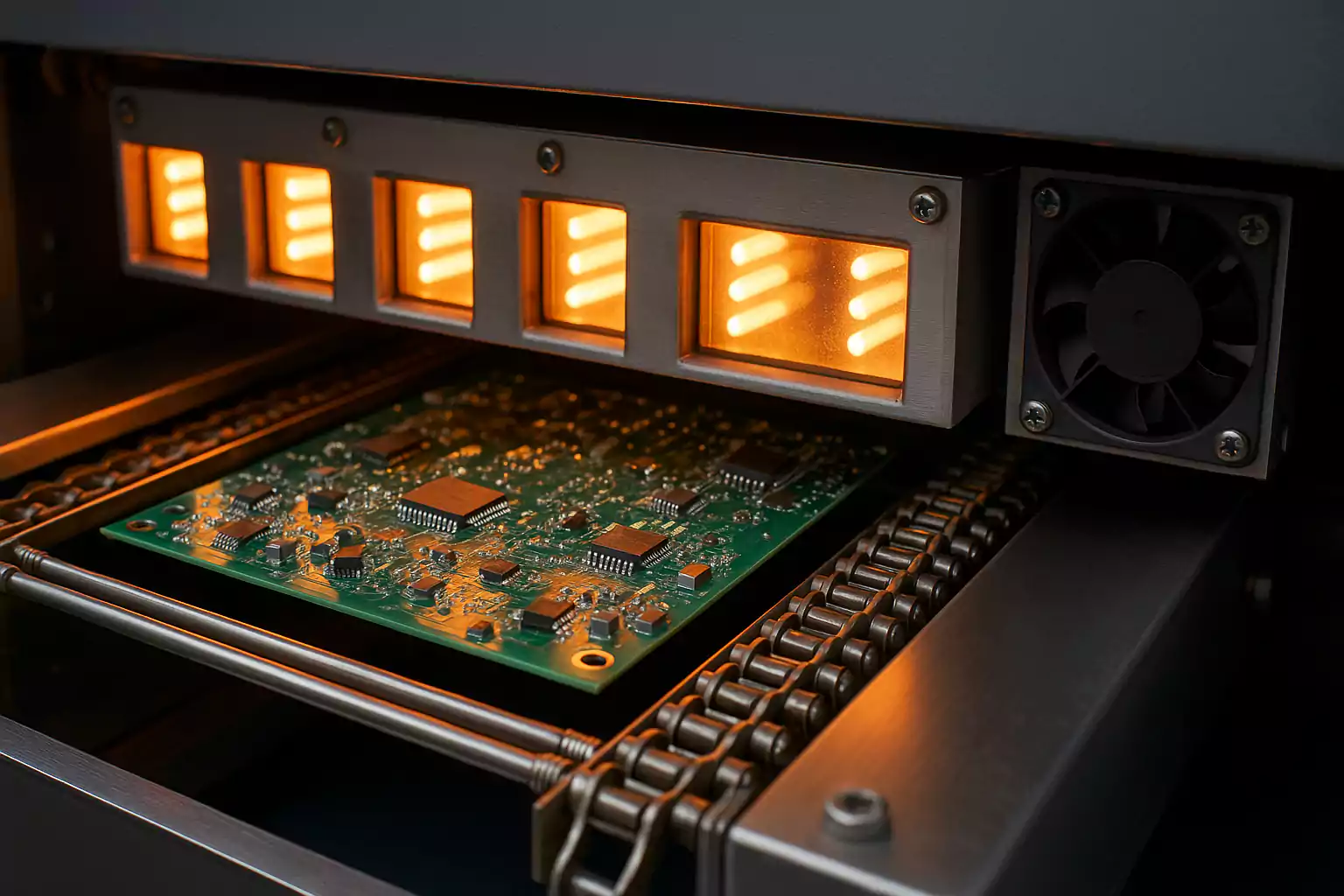
The key objective of reflow soldering is to ensure consistent, high-quality solder joints while minimizing thermal damage to components. It involves precisely controlled heating and cooling cycles that melt and solidify solder paste in a repeatable manner. This is achieved using specialized equipment known as reflow ovens, which feature multiple temperature zones, conveyor systems, and often inert atmospheres for better joint reliability.
In an era of miniaturized electronics and high-density PCB layouts, reflow soldering plays a critical role in ensuring product performance, durability, and cost-efficiency. It’s also essential for lead-free electronics manufacturing, complying with environmental standards like RoHS.
This in-depth guide will walk you through every aspect of the reflow soldering process—from temperature profiles and equipment types to common defects and proven best practices—so that you can fully understand and optimize your SMT production.
Overview of the Reflow Soldering Process
Reflow soldering is a thermal process used to permanently attach surface-mount components (SMDs) to the pads of a printed circuit board (PCB) by heating solder paste until it melts, flows, and solidifies. It is the most widely used soldering technique in automated SMT (Surface Mount Technology) assembly lines due to its repeatability, compatibility with fine-pitch components, and ability to handle complex board layouts.
How It Works — Step by Step
- Solder Paste Application
The process begins with stencil printing, where solder paste—a mixture of powdered solder alloy and flux—is applied onto the PCB pads using a metal stencil. The flux helps remove surface oxides and promotes solder wetting during heating. - Component Placement
Surface-mount components are accurately placed on the solder-pasted pads using a pick-and-place machine. The tackiness of the solder paste holds the components in position temporarily. - Preheat and Thermal Profiling
The loaded PCB is transported into a reflow oven, which is divided into multiple heating zones. The board is gradually heated to prepare it for soldering, with temperatures controlled according to a reflow profile to avoid thermal shock. - Reflow (Peak Heating)
Once the solder reaches its melting point (typically 217–245 °C for lead-free alloys), it becomes liquid and forms metallurgical bonds between the component leads and PCB pads. This is the critical reflow phase. - Cooling
After the peak temperature is reached, the board enters a controlled cooling zone, where the molten solder solidifies into strong, reliable joints.
Why Reflow Is So Widely Used
- Automation-Friendly: Reflow soldering integrates seamlessly into high-speed SMT production lines.
- Precision: Ideal for small pitch components like BGAs, QFNs, and 0201 resistors.
- Lead-Free Compatibility: Easily adaptable to RoHS-compliant, lead-free solder alloys.
- Repeatability: Thermal profiles can be tightly controlled to ensure uniform results.
Whether assembling consumer electronics or mission-critical aerospace systems, reflow soldering offers the balance of efficiency, control, and reliability that modern electronics demand.
Reflow Soldering Equipment & System Structure
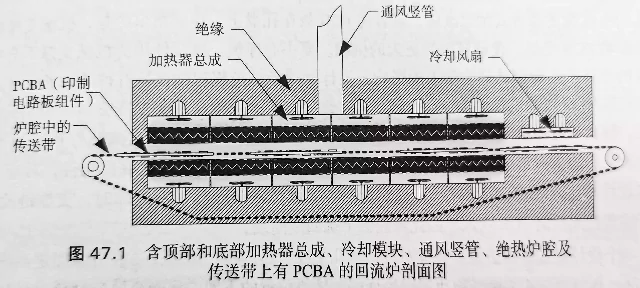
To achieve precise thermal control and high-throughput SMT assembly, reflow soldering relies on a specialized piece of machinery known as a reflow oven. These ovens are designed to heat PCBs uniformly through multiple thermal zones while transporting the boards via a conveyor system. Understanding the internal structure and operating principles of reflow ovens is essential for optimizing soldering performance and minimizing defects.
Key Components of a Reflow Oven
Most industrial reflow ovens consist of the following subsystems:
- Heating Modules
Located above and below the conveyor belt, these modules deliver controlled thermal energy through either convection, infrared radiation, or a combination of both. Modern ovens typically feature multiple heating zones (e.g., 6 to 12), each independently controlled for precise temperature profiling. - Thermal Zones
Divided into preheat, soak, reflow, and cooling zones. Each section gradually raises or lowers the temperature to match the programmed reflow profile. - Conveyor System
Transports PCBs through the oven. Two common types:- Edge-hold chain conveyor: Holds the board by its edges with metal fingers (ideal for rigid PCBs without edge components).
- Mesh belt conveyor: Supports the PCB from underneath (better for flexible boards or assemblies with overhanging parts).
- Exhaust System
Removes flux fumes and gases generated during heating, preventing contamination and improving air quality inside the oven chamber. - Cooling Section
Rapidly lowers the PCB temperature to solidify solder joints and reduce the risk of grain growth or microcracks.
Heating Technologies in Reflow Ovens
Reflow ovens employ different heating methods to achieve solder melting. Each has its own advantages and limitations:
- Infrared (IR) Heating
Uses IR lamps to radiate heat onto the PCB. Efficient and simple, but prone to uneven heating due to varying absorption rates of different components and board materials. - Forced Convection Heating
The most common method in modern reflow ovens. Hot air is circulated to ensure uniform heating across the entire board, regardless of color, size, or component type. - Vapor Phase Reflow (less common)
Immerses the PCB in a dense vapor of inert fluid. The vapor condenses on the board, releasing latent heat. Extremely uniform but expensive and less scalable. - Hybrid Systems
Some ovens combine IR and convection for optimized heating—providing fast ramp-up with better thermal uniformity.
Conveyor System Comparison: Chain vs. Mesh Belt
| Feature | Chain Conveyor | Mesh Belt Conveyor |
|---|---|---|
| Contact Point | Grabs PCB edges | Supports full PCB bottom |
| Component Clearance | Best for edge-free designs | Supports overhanging parts |
| Cleaning & Maintenance | Low contamination risk | May trap flux residues |
| Application | High-rigidity boards | Flexible or irregular PCBs |
Choosing the right transport method depends on PCB design, component placement, and production needs.
Reflow oven configuration directly impacts soldering consistency, throughput, and long-term yield. Engineers must understand the strengths and trade-offs of each oven type and configuration to match their manufacturing goals.
The Ideal Reflow Temperature Profile
A reflow temperature profile is the thermal recipe that controls how a PCB is heated and cooled as it passes through a reflow oven. It is arguably the most critical factor in ensuring strong, reliable solder joints and avoiding thermal damage to components or substrates.
The profile defines the temperature vs. time curve, and typically consists of four distinct zones: preheat, soak, reflow, and cooling. Each zone must be carefully tuned based on the PCB layout, component mix, and type of solder paste used.
The Four Key Reflow Zones
1. Preheat Zone
- Purpose: Gradually raises the temperature of the PCB to prevent thermal shock and prepare the solder paste for activation.
- Ramp Rate: Typically 1–3 °C/s (max 4 °C/s). Faster ramps may cause component cracking or solder spatter.
- Target Temp: Usually 100–150 °C, depending on paste formulation and board density.
2. Soak Zone (Thermal Equilibrium)
- Purpose: Allows the board and components to reach a uniform temperature. Flux is activated here to remove oxides.
- Dwell Time: Typically 60–120 seconds
- Temperature Range: Between 140–180 °C
- Soak profiles also help reduce cold joints and improve wetting.
3. Reflow (Peak) Zone
- Purpose: Heat the solder paste above its liquidus temperature (typically 217 °C for SAC305) so it fully melts and creates metallurgical bonds.
- Peak Temperature: Generally 240–250 °C for lead-free solder
- TAL (Time Above Liquidus): Should be maintained for 30–90 seconds depending on the paste. Excessive TAL can cause intermetallic layer overgrowth, reducing joint reliability.
4. Cooling Zone
- Purpose: Solidifies solder joints and prevents grain coarsening.
- Cooling Rate: Ideally 2–4 °C/s
- Too fast = thermal shock, too slow = brittle joints
Common Reflow Profile Types
Two widely used profile formats are:
1.Ramp-Soak-Spike (RSS)
- Most common for complex assemblies
- Smooth ramp → extended soak → quick spike to peak temp
- Better for thermal uniformity and flux activation
2.Ramp-to-Spike (RTS)
- Simplified profile with a continuous ramp up to peak
- Faster process, but riskier for large thermal mass boards
Visualizing the Temperature Curve
A typical lead-free reflow curve looks like this:
- Gradual preheat from ambient to ~150 °C
- Soak plateau between 150–180 °C
- Sharp rise to 240–250 °C
- Rapid controlled cooling
Key Parameters to Monitor
| Parameter | Target Range | Notes |
|---|---|---|
| Ramp rate | 1–3 °C/s | Avoid cracking or flux boiling |
| Soak duration | 60–120s | Promotes thermal uniformity |
| Peak temp | 240–250 °C (lead-free) | Avoid exceeding component specs |
| Time above liquidus | 30–90s | Crucial for intermetallic layer control |
| Cooling rate | 2–4 °C/s | Avoid microcracks |
Profiling tools (like thermocouples and profiler loggers) are essential for validating and adjusting your reflow oven settings. No two boards are exactly the same—customizing your temperature curve is the key to achieving consistent, high-quality results.
Lead-Free Reflow: Process Changes and Challenges
The global shift toward environmentally friendly electronics has made lead-free reflow soldering the new industry standard. Driven by regulatory frameworks such as the EU RoHS Directive, manufacturers have transitioned from traditional tin-lead (Sn63/Pb37) solder to lead-free alloys, most commonly SAC305 (Sn96.5/Ag3.0/Cu0.5).
However, this shift introduces several important changes to the reflow process—and new challenges that engineers must carefully manage to ensure solder joint reliability and long-term product performance.
Key Process Differences: Lead-Free vs. Leaded Reflow
| Parameter | Leaded Reflow (SnPb) | Lead-Free Reflow (SAC305) |
|---|---|---|
| Liquidus Temperature | ~183 °C | ~217 °C |
| Peak Temperature | ~210–220 °C | ~240–250 °C |
| Time Above Liquidus | 30–60 seconds | 30–90 seconds |
| Flux Activity Level | Moderate | Higher required |
| Process Window | Wider | Narrower / tighter control |
| IMC (Intermetallic) Growth | Slower | Faster |
Lead-Free Reflow Challenges
1. Higher Peak Temperatures
Lead-free solder pastes like SAC305 require reflow peak temperatures of 240–250 °C, significantly higher than the ~215 °C used in leaded processes. This increases:
- Thermal stress on components and PCB substrates
- Risk of delamination, component cracking, and warping
- Need for heat-tolerant materials and precise thermal profiling
2. Narrower Process Window
Lead-free soldering has less margin for error. Too little heat can lead to cold joints, while excessive TAL (Time Above Liquidus) can cause:
- Excessive intermetallic compound (IMC) layer growth, making joints brittle
- Component oxidation or flux burnout
3. Solder Joint Appearance
Lead-free joints typically appear dull or grainy compared to the shiny finish of leaded solder. While not a quality issue, it can cause confusion during visual inspection without proper training.
4. More Aggressive Flux Required
Higher temperatures increase oxidation. As a result, stronger flux chemistry is required to clean surfaces and ensure proper wetting. However, aggressive fluxes may leave residues and require post-solder cleaning in sensitive applications.
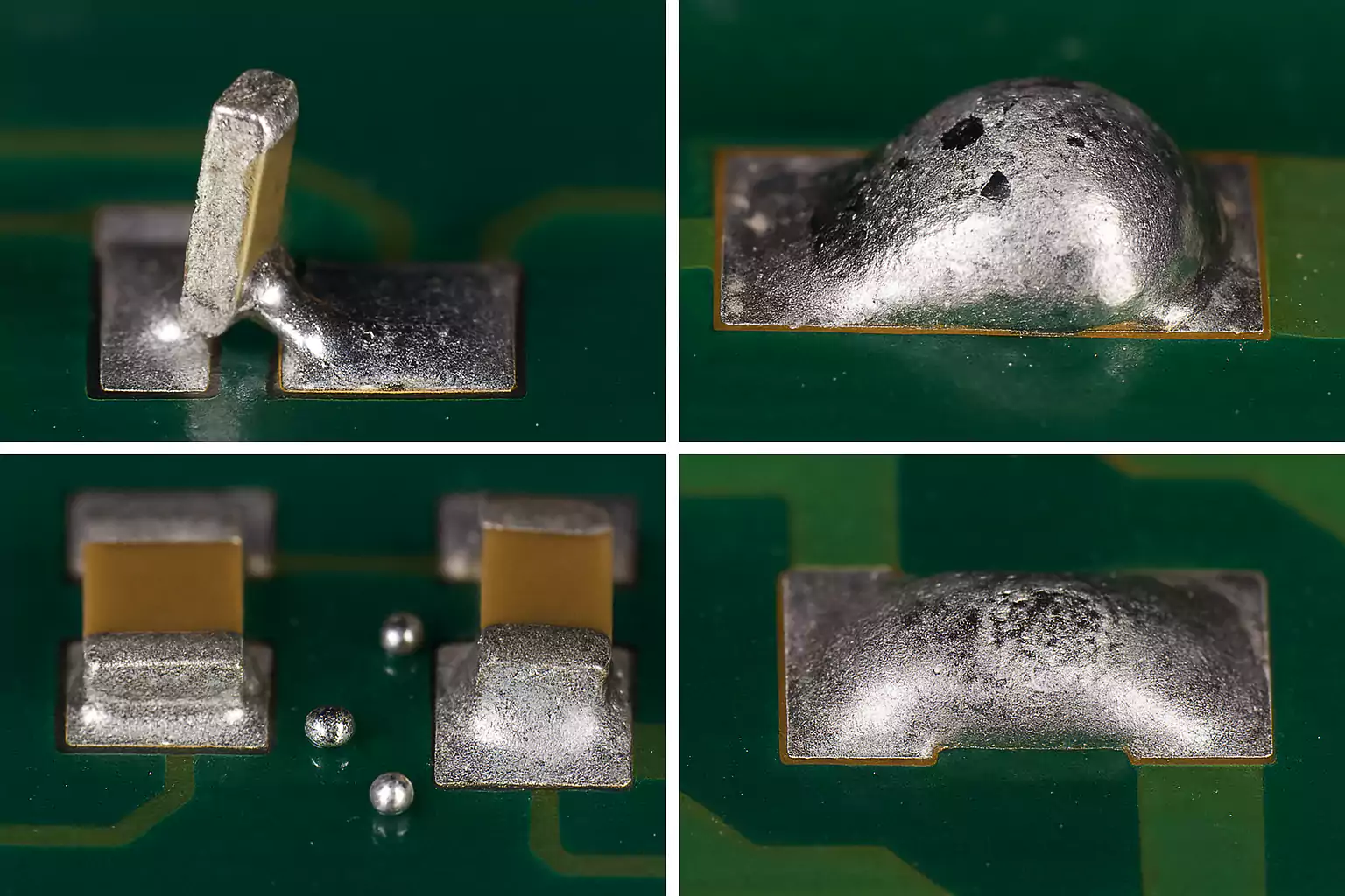
Common Reflow Defects and How to Prevent Them
Even with a well-calibrated reflow profile, defects can occur due to variations in PCB design, solder paste quality, or environmental factors. Below are the most common reflow soldering issues, along with actionable strategies to prevent them.
1.Tombstoning
What it is: One end of a chip component lifts vertically from the PCB, resembling a tombstone.
Cause: Uneven wetting forces due to temperature imbalance or paste volume inconsistency.
Prevention:
- Ensure symmetrical pad design
- Use consistent solder paste volume
- Optimize soak zone for better thermal balance
2.Voids in Solder Joints
What it is: Trapped gas pockets within the solder joint, weakening mechanical strength and thermal conductivity.
Cause: Poor paste outgassing, excessive flux residue, or fast reflow ramp rate.
Prevention:
- Use low-voiding solder paste
- Apply vacuum reflow or nitrogen atmosphere if possible
- Maintain proper preheat and soak times to promote flux evaporation
3.Solder Balling
What it is: Small, unwanted solder spheres scattered around pads or traces.
Cause: Spattering from rapid heating or poor stencil cleaning.
Prevention:
- Reduce ramp rate during preheat
- Improve stencil wiping and board cleanliness
- Avoid excess solder paste deposition
4.Cold Joints
What it is: Dull, brittle solder joints indicating incomplete melting or wetting.
Cause: Insufficient peak temperature or too short TAL.
Prevention:
- Verify thermal profile meets solder paste specs
- Increase reflow zone temperature if needed
- Confirm even heat distribution across PCB
5.Graping
What it is: Granular or oxidized appearance of solder joints, resembling a bunch of grapes.
Cause: Oxidation of fine solder particles before full reflow.
Prevention:
- Reduce soak time and avoid long TAL
- Use paste with larger solder powder and stable flux chemistry
- Minimize delays between printing and reflow
6.Component Shifting or Skew
What it is: SMD components move out of alignment during reflow.
Cause: Imbalanced wetting or vibration during paste liquefaction.
Prevention:
- Ensure consistent solder paste application
- Use anti-skew pad design
- Stabilize conveyor speed and reduce oven vibrations
Defect prevention in reflow soldering is all about process control. By regularly profiling ovens, monitoring solder paste behavior, and analyzing board layouts, manufacturers can significantly reduce defect rates and improve first-pass yield.
Reflow Best Practices: Process Optimization Tips
Achieving high-yield, defect-free SMT soldering requires more than just a functional reflow oven. It takes attention to detail across solder paste handling, board design, thermal profiling, and equipment maintenance. The following best practices help ensure reliable solder joints and consistent manufacturing results.
1. Calibrate and Maintain Reflow Equipment
Regularly inspect and calibrate your reflow oven's temperature zones, conveyor speed, and airflow consistency. Even slight deviations in zone temperatures can lead to cold joints or excessive intermetallic growth.
2. Choose the Right Solder Paste
Select solder paste based on your application—lead-free (e.g., SAC305) or leaded, type of flux (no-clean, water-soluble), and alloy composition. Check paste specifications for:
- Optimal TAL (Time Above Liquidus)
- Peak reflow temp range
- Shelf life and stencil life
3. Optimize PCB Design for Reflow
Design with DFM (Design for Manufacturability) in mind:
- Keep pad sizes consistent with component specs
- Minimize thermal mass imbalance
- Use non-solder-mask-defined (NSMD) pads for better wetting
- Include fiducials for accurate pick-and-place alignment
4. Create a Reflow Profile per Assembly
Each PCB layout, component set, and solder paste may require a custom thermal profile. Use profiling tools to measure:
- Ramp rate
- Soak duration
- Peak temp
- Time above liquidus
- Cooling rate
5. Manage Moisture-Sensitive Components
Many SMD packages (like BGAs, QFNs, and plastic connectors) are MSL-rated and prone to popcorning or delamination under high reflow heat if moisture is present.
6. Control Cleanliness and Handling
Flux residues, fingerprints, and dust can interfere with wetting and inspection. Implement:
- Clean work surfaces and gloves
- Scheduled stencil cleaning
- PCB baking to remove moisture and oils
7. Use In-Line Inspection and Feedback Loops
Post-reflow AOI (Automated Optical Inspection) and X-ray inspection for BGAs help catch defects early. Feed inspection results back into profiling or design improvements.
Reflow soldering is not a "set-it-and-forget-it" process. Continuous monitoring, feedback, and fine-tuning are the pillars of a high-yield SMT operation.
How to Create and Adjust Reflow Profiles
Creating an effective reflow temperature profile is one of the most critical tasks in SMT assembly. A well-optimized profile ensures solder paste melts and solidifies under ideal thermal conditions, reducing defects and improving long-term reliability.
Each PCB assembly may require a custom profile based on solder paste type, board thickness, component density, and material thermal mass.
Step-by-Step: Creating a Reflow Profile
1. Understand the Solder Paste Requirements
Begin by reviewing the solder paste technical datasheet. Manufacturers specify:
- Recommended ramp rate
- Soak and reflow temperature ranges
- Time Above Liquidus (TAL)
- Maximum peak temperature
- Acceptable cooling rate
2. Select Thermocouple Locations
Place 3 to 5 thermocouples (TCs) on the PCB at:
- Heaviest thermal mass component (e.g., large inductors)
- Smallest and most heat-sensitive device
- Center of the board
- Edge zone
- Under BGA (optional, using drilled vias or embedded sensors)
3. Run the First Trial Profile
Pass the board through the oven while recording temperature data from each TC. Most reflow profiling systems include:
- Real-time temp graphs
- Zone control summaries
- Deviation alerts for TAL, peak, and ramp rate
4. Analyze the Profile Curve
Compare the captured curve to the paste spec:
- Is the ramp rate between 1–3 °C/s?
- Is TAL within the specified time?
- Does peak temperature reach target range?
- Are all zones heating uniformly?
5. Make Adjustments and Fine-Tune
If the profile deviates:
- Adjust conveyor speed to change time exposure
- Raise/lower zone temps as needed
- Shift zone boundaries to increase/decrease soak time
6. Validate with Inspection
After finalizing the profile, run a batch and perform:
- Visual inspection (wetting, fillet formation)
- X-ray inspection (BGA voids, head-in-pillow)
- Pull/shear tests for mechanical strength (if required)
Only after confirming joint quality should the profile be released for production.
Reflow Profiling: Best Practice Reminders
- Re-profile when changing paste, board stack-up, or component mix
- Revalidate profiles after oven maintenance or repair
- Store profiles digitally by board revision, paste lot, and date
Thermal profiling bridges the gap between theory and practice in reflow soldering. It transforms soldering from a trial-and-error task into a data-driven, repeatable process.
Frequently Asked Questions (FAQ): Reflow Soldering
What is Time Above Liquidus (TAL) in reflow soldering?
TAL refers to the amount of time the solder is maintained above its liquidus temperature (usually ~217 °C for lead-free SAC305 alloys). This period is critical to ensuring the solder fully melts, wets the pads, and forms strong metallurgical bonds. Too short a TAL can result in cold joints, while too long can cause excessive intermetallic growth, weakening the solder joint.
Ideal TAL for SAC305: 30–90 seconds
What is the difference between RSS and RTS reflow profiles?
·RSS (Ramp-Soak-Spike) profiles gradually heat the PCB, allow a thermal soak, and then spike to reflow temperature. They offer better thermal uniformity and are ideal for complex boards.
·RTS (Ramp-To-Spike) profiles skip the soak phase and go directly to reflow temperature. They’re faster but can risk uneven heating.
How do I prevent tombstoning during reflow?
Tombstoning occurs when one side of a small component lifts off the pad due to uneven soldering forces. To prevent it:
·Ensure equal solder volume on both pads
·Maintain thermal symmetry
·Avoid overly fast ramp rates
·Optimize pad design and spacing
What is the ideal peak temperature for SAC305?
For lead-free SAC305 solder paste, the typical peak reflow temperature is between 240 °C and 250 °C. This ensures complete melting and sufficient wetting while staying within component temperature tolerances (usually ≤260 °C per JEDEC J-STD-020).
Can I use the same profile for all PCBs?
No. Each PCB may differ in thickness, copper distribution, and component types. A custom reflow profile should be created and validated for each unique assembly. Use thermocouples to measure temperature in key areas and adjust the oven zones accordingly.
What causes solder voids and how can I reduce them?
Solder voids are trapped gas bubbles inside joints. Causes include:
·Excess flux residue
·Poor outgassing during reflow
·Inadequate preheat or soak
To reduce voids:
·Use low-voiding solder paste
·Add a vacuum reflow step if possible
·Optimize preheat to allow complete solvent evaporation
Is nitrogen atmosphere necessary for reflow?
While not mandatory, nitrogen reflow can significantly improve joint quality by reducing oxidation. It's especially useful for:
·Lead-free soldering
·Fine-pitch components (e.g., BGA, QFN)
·High-reliability applications (e.g., aerospace, medical)
How often should I re-profile my reflow oven?
You should re-profile when:
·Changing solder paste brand/type
·Switching PCB layout or component density
·After maintenance or oven recalibration
·Periodically, as part of quality control (e.g., monthly)
Conclusion: Getting Reflow Soldering Right
Reflow soldering is a complex but essential process at the heart of modern PCB assembly. When properly controlled, it delivers strong, reliable solder joints that can withstand the electrical and mechanical stresses of today's high-density electronic designs.
Throughout this guide, we've explored the full spectrum of reflow soldering—from oven structure and temperature profiling to common defects and best practices. Whether you're working with leaded or lead-free solder, success depends on balancing multiple variables: thermal profile, solder paste chemistry, board design, and component handling.