


Printed Circuit Board Assembly (PCBA) plays a pivotal role in the world of electronics manufacturing. Think of PCBA as the essential step that brings a PCB to life, making it ready for use in everything from consumer gadgets to complex medical equipment.
In this article, we'll break down PCBA—its definition, types, processes, and quality control—giving you a clear understanding of how important it is in today's electronics industry.
Definition
What Is PCBA?
Printed Circuit Board Assembly (PCBA) refers to the process of mounting and soldering electronic components onto a printed circuit board (PCB) to create a functional electronic assembly.
A PCBA not only includes the bare board itself but also all the resistors, capacitors, connectors, and integrated circuits that deliver the final device's functionality.
What Is PCB Assembly?
PCB Assembly is the broader term for the end-to-end activities required to transform a bare PCB into a working electronic module.
This process encompasses stencil printing of solder paste, placement of surface-mount and through-hole components, reflow or wave soldering, and post-solder inspections.
In industry parlance, "PCBA" and "PCB assembly" are often used interchangeably, but PCBA focuses on the result—the assembled board—PCB assembly covers each step in the production line, including design for manufacturability (DFM), pick-and-place programming, and final functional testing.
Difference Between PCB and PCBA
When comparing a bare PCB to a fully assembled PCBA, the distinction is clear:
| Aspect | PCB (Printed Circuit Board) | PCBA (PCB Assembly) |
| Definition | An insulated board with etched copper traces | A PCB populated with electronic components and soldered connections |
| Components | Copper layers, substrate, solder mask, silkscreen | All passive and active electronic parts (ICs, resistors, capacitors, connectors) |
| Functionality | Provides electrical pathways only | Performs the intended electronic functions of the device |
| Manufacturing Steps | Fabrication: lamination, etching, drilling | Fabrication + assembly: solder paste printing, placement, soldering, testing |
| Testing | Often electrical continuity tests | In Circuit Test (ICT), Functional Test, X ray inspection, AOI |
Historical Development of PCBA
The roots of PCBA trace back to the 1950s, when early electronic circuits were hand-wired point-to-point. The invention of the printed circuit board in 1956 revolutionized electronics by etching conductive pathways on insulating substrates.
In the 1960s and 1970s, through-hole technology (THT) became standard for mounting bulky components. The 1980s saw the introduction of Surface Mount Technology (SMT), which allowed for higher component density and automated pick-and-place machines.
Over the past four decades, continual innovations in reflow soldering, automated optical inspection (AOI), and design-for-manufacturability (DFM) software have driven PCBA toward ever-smaller, more reliable, and cost-effective assemblies—paving the way for today's compact smartphones, wearables, and Internet of Things devices.
PCBA Types: Comparison Overview
To help you quickly compare the main PCBA methods and decide which best fits your project needs, here is an at-a-glance overview:
| Type | Process Principle | Component Package | Typical Applications | Advantages | Disadvantages |
| Surface Mount Technology (SMT) | Solder paste printed on pads → placement of SMDs → reflow soldering | Surface mount devices (SMD) | Smartphones, laptops, wearables | High component density; fully automated | Requires precise pad design; small parts handling |
| Through Hole Technology (THT) | Leaded components inserted through plated holes → wave soldering | Pluggable components (PTH) | Power supplies, connectors, military | Excellent mechanical strength; robust joints | Lower density; slower, more labor intensive |
| Hybrid Technology (SMT + THT) | Combines SMT reflow and THT insertion/wave solder | Mixed SMD and PTH | Industrial controls, medical devices | Balances density with mechanical strength | Higher line complexity; increased setup cost |
Advanced PCB Assembly Techniques
In addition to the core SMT, THT, and hybrid methods, modern electronics often leverage specialized assembly approaches to meet unique space, performance, or reliability requirements:
- Micro-BGA and Fine-Pitch SMT
Ultra-small solder ball arrays enable very high pin-count ICs to be mounted in compact footprints. Common in smartphones and high-speed computing modules.
- 3D PCB Assembly
Boards are stacked or folded to create three-dimensional structures, maximizing functionality in constrained volumes—ideal for wearables and compact IoT devices.
- Chip-On-Board (COB)
Bare silicon dies are directly bonded and wire-bonded onto the PCB, then encapsulated. This technique reduces component height and improves signal integrity.
- Ball-Grid Array (BGA)
BGA packages sit on a grid of solder balls, providing excellent thermal performance and electrical connectivity for high-pin-count devices used in servers and advanced controllers.
Each of these advanced techniques fills a specific niche—highlighting the importance of selecting the right assembly method to balance size, performance, cost, and reliability in your final product.
PCB Assembly Process
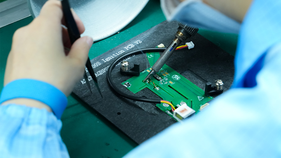
By following a series of standardized PCB assembly steps—from solder-paste printing to final inspection—manufacturers ensure reliable electrical connections, optimal performance, and consistent product quality.
Understanding this end-to-end workflow is essential for design engineers, procurement specialists, and anyone sourcing PCB assembly services.
Step-by-Step PCB Assembly Flow
1. Design for Manufacturability (DFM) Review
Engineers validate the PCB layout against manufacturing constraints (clearances, pad sizes, thermal reliefs).
2. Solder Paste Application
A steel stencil deposits a uniform layer of solder paste onto each copper pad.
3. Pick-and-Place
High-speed machines accurately position surface-mount devices (SMDs) onto the pasted pads.
4. Reflow Soldering
The board passes through a controlled-temperature reflow oven, melting solder and forming permanent joints.
5. Through-Hole Insertion & Wave/Selective Soldering
For through-hole components, leads are inserted and soldered via a wave or selective process.
6. Cleaning & Flux Removal
Any residual flux is cleaned—often with aqueous or solvent methods—to prevent corrosion.
7. Inspection & Testing
Automated Optical Inspection (AOI), X-ray, In-Circuit Test (ICT), and Functional Test verify solder integrity and circuit functionality.
How PCBA Fits into Electronics Manufacturing
PCBA is the bridge between bare-board fabrication and finished electronic products. By integrating component mounting, soldering, and testing into a streamlined production line, PCB assembly enables high volume, consistent quality, and fast time-to-market. Key advantages include:
- Scalability: Adaptable throughput from prototypes to mass production
- Cost Efficiency: Reduced manual labor and rework
- Reliability: Automated inspection minimizes defects
Key Tools and Equipment in PCB Assembly
| Equipment | Function |
| Solder Paste Printer | Applies precise solder paste deposits |
| Pick and Place Machine | Rapid placement of SMD components |
| Reflow Oven | Melts solder paste under controlled thermal profile |
| Wave/Selective Soldering | Solder through hole components |
| Automated Optical Inspection | Detects missing parts, tombstoning, solder bridges |
| In Circuit Test (ICT) Rig | Electrically tests individual nets and components |
Role of CAD Software in PCB Design and Assembly
CAD software sits at the heart of the PCB assembly process, offering tools for schematic capture, layout editing, and DFM rule checking. Modern PCB CAD platforms generate pick-and-place data, stencil artwork, and Gerber files that drive every downstream assembly step.
By catching layout errors early and automating data export for stencil printers and pick-and-place machines, CAD integration slashes lead times and reduces miscommunication between design and manufacturing teams.
Key Benefits of PCBA
Automation and Precision
By leveraging automated pick-and-place machines and reflow soldering ovens, PCBA delivers placement accuracy down to ±0.01 mm and repeatable solder joint quality.
This level of automation minimizes human error, increases throughput (often exceeding 20,000 CPH—components per hour), and ensures consistent alignment of fine-pitch components.
Cost Efficiency and Scalability
- Reduced Labor Costs: Automated lines cut manual soldering and inspection labor by up to 70%.
- Economies of Scale: Unit cost drops significantly with volume—often 30–50% cheaper at 10,000+ units versus prototypes.
- Flexible Batch Sizes: Same process handles one-off prototypes and full production runs without retooling.
Improved Quality and Reliability
| Quality Measure | Benefit |
| Automated Optical Inspection (AOI) | Detects > 99% of solder defects (bridges, tombstoning) |
| In Circuit Test (ICT) | Verifies > 95% of component nets before functional testing |
| X Ray Inspection | Identifies hidden BGA and fine pitch solder joint issues |
| Controlled Reflow Profiles | Ensures consistent solder paste wetting and reduces void rate |
Environmental Advantages
Modern PCBA lines use lead-free solders (e.g., SAC305 alloy) and closed-loop solvent systems, reducing hazardous waste by over 60% compared to legacy processes.
Water-jet or ultrasonic cleaning recycles 80% of rinse water, supporting RoHS and WEEE compliance while lowering disposal costs.
Accelerated Time-to-Market
- Rapid Prototyping: Integrated stencil and pick-and-place data from CAD allow first-article builds within 24–48 hours.
- Concurrent Processes: DFM review, stencil setup, and placement programming run in parallel to fabrication.
- Streamlined Supply Chain: Vendor-managed inventory (VMI) for components reduces lead times by up to 40%.
PCBA Testing
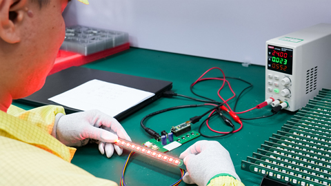
Importance of Testing in PCB Assembly
Effective PCBA testing is critical to guarantee product reliability, reduce field failures, and comply with industry standards.
By integrating testing at multiple stages, manufacturers can detect assembly defects—such as solder bridges, opens, and misalignments—before boards leave the factory. This not only minimizes costly recalls but also strengthens customer trust in your brand.
Key Types of PCBA Tests
1. Automated Optical Inspection (AOI)
- Uses high-resolution cameras to scan solder joints and component placement.
- Typical defect coverage: > 99% detection of missing parts, tombstoning, and solder bridges.
2. In-Circuit Test (ICT)
- Applies test probes to individual nets to verify component values, shorts, and opens.
- Coverage: checks resistors, capacitors, diodes, and digital ICs before functional testing.
3. X-Ray Inspection
- Non-destructive imaging to inspect hidden solder joints (e.g., BGA, QFN).
- Ideal for verifying solder ball integrity and detecting voids.
4. Flying Probe Test
- Flexible test heads move over the board to contact nets without custom fixtures.
- Cost-effective for prototypes and small batches with moderate coverage.
5. Functional Test
- Powers up the board in a simulated operating environment to validate end-use performance.
- Can include signal-integrity checks, communication interfaces, and power-on sequences.
6. Burn-In Test
- Stresses assemblies under elevated temperature and voltage for extended periods.
- Reveals early-life failures and marginal solder joints before shipment.
Common Testing Challenges and Solutions
| Challenge | Solution |
| False fails in AOI due to poor lighting | Calibrate cameras; adjust lighting and contrast parameters |
| Fixture cost for ICT on low volume boards | Use flying probe test or modular ICT fixtures to reduce tooling |
| Inspecting hidden joints under BGA/POG | Implement X ray inspection or boundary scan techniques |
| Incomplete functional coverage | Develop comprehensive test scripts; include edge case scenarios |
| High test cycle time | Optimize parallel test stations; batch similar boards together |
Role of DFM in Enhancing Testability
Design for Manufacturability (DFM) directly impacts how effectively a board can be tested. Early DFM reviews identify problematic footprints, inaccessible test points, and tight spacing that hinder fixture design or probe access.
By prioritizing testability during the layout phase, you can:
- Ensure Access to Test Points: Include clearly labeled vias and pads for probe contacts.
- Standardize Footprints: Use common component packages to simplify ICT fixture design.
- Optimize Component Placement: Maintain minimum spacing between pads and components for reliable AOI and soldering.
- Plan for Boundary Scan: Incorporate JTAG headers on complex digital boards to enable non-intrusive chain testing.
PCBA Quality Control
Quality Assurance Methods in PCBA
Effective quality assurance (QA) in PCB assembly combines inline process controls with post-assembly inspections to catch defects early and maintain consistent yield.
Key QA methods include Solder Paste Inspection (SPI) to verify paste volume, Automated Optical Inspection (AOI) for component placement and solder-joint quality, In-Circuit Test (ICT) for electrical connectivity, and Functional Test for end-use performance.
By integrating these checks into the PCB assembly line, manufacturers reduce rework rates and ensure each board meets stringent reliability criteria.
Industry Standards and Best Practices
- IPC-A-610 (Acceptability of Electronic Assemblies): Defines workmanship criteria for solder joints and component placement.
- IPC-6012 (Qualification and Performance Specifications): Specifies performance requirements for rigid PCBs and assemblies.
- ISO 9001: Framework for implementing a robust quality management system across the organization.
- RoHS & REACH Compliance: Ensures lead-free solder and restricted-substance adherence.
- Statistical Process Control (SPC): Monitors key process parameters (temperature, humidity, solder paste volume) to maintain process stability.
- Regular Equipment Calibration: Scheduled calibration of printers, pick-and-place machines, and ovens to prevent drift.
How to Ensure a High-Quality PCBA
- Select High-Quality Materials: Use certified PCB substrates, solder pastes, and components from approved vendors.
- Implement DFM Reviews: Early design checks reduce risky footprints and improve solderability.
- Establish Process Controls: Define and document process windows for stencil printing, placement accuracy, and reflow profiles.
- Monitor with SPC: Track key metrics in real time (e.g., solder paste volume, component placement variance).
- Conduct Regular Audits: Schedule line-side audits and first-article inspections to catch deviations.
- Empower Continuous Improvement: Analyze defect data, run root-cause analyses, and update work instructions.
Common Defects in PCBA and How to Avoid Them
| Defect | Prevention |
| Solder bridges | Optimize stencil apertures; adjust solder paste volume |
| Tombstoning of small components | Fine tune reflow profile; ensure balanced pad design |
| Insufficient solder wetting | Verify paste rheology; maintain oven temperature profile |
| Component misplacement | Calibrate pick and place machines; implement AOI feedback loops |
| Void formation in BGA joints | Adjust pre heat zone; use vacuum or nitrogen assisted reflow ovens |
Importance of Traceability in Quality Control
Traceability in PCBA ensures every board's production history—from raw materials to final test—can be tracked and audited. This capability is critical for managing recalls, analyzing failure trends, and demonstrating compliance to regulators and customers.
Key traceability practices
- Lot and Batch Coding: Assign unique codes to solder paste, components, and PCB panels.
- Serial Numbering: Label finished assemblies for individual board tracking.
- Digital Record-Keeping: Use Manufacturing Execution Systems (MES) to log process parameters and inspection results.
- Component History Reports: Maintain certificates of conformance (CoCs) and supplier quality data.
PCBA Applications
Industries That Use PCBA
- Consumer Electronics: Smartphones, tablets, laptops, game consoles—where high-density SMT assemblies enable compact, feature-rich devices.
- Automotive: Engine control units (ECUs), infotainment systems, ADAS sensors—requiring robust PCBA capable of withstanding vibration and temperature extremes.
- Industrial Automation: PLCs, motor drives, robotics controllers—demanding hybrid PCBA for both high-density logic and heavy-duty power components.
- Telecommunications: 5G base station modules, network routers, optical transceivers—leveraging advanced BGA and fine-pitch SMT for high-speed data processing.
- Aerospace & Defense: Avionics, radar systems, missile guidance—where stringent quality control and traceability are mandatory.
- Medical Devices: Patient monitors, infusion pumps, diagnostic equipment—requiring biocompatible coatings and rigorous functional testing.
Examples of Products Relying on PCBA
| Product Category | Role of PCBA |
| Wearable Fitness Trackers | Miniaturized SMT assemblies for sensors, microcontrollers, and wireless modules |
| Smart Home Hubs | Hybrid PCBA integrating power supplies, Wi Fi radios, and MCU logic |
| Electric Vehicle Inverters | High current THT components for power conversion alongside SMT control circuitry |
| Network Switches | Fine pitch BGA for high density port controllers and FPGA chips |
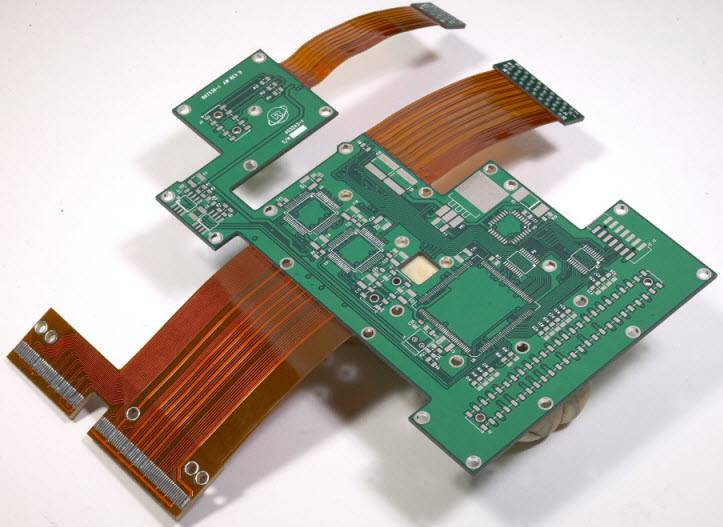
| Portable Ultrasound Units | Rigid flex PCBA combining rigid logic boards with flexible transducer interfaces |
Innovative Applications of PCBA in Emerging Industries
Emerging sectors push PCBA technology beyond traditional boundaries, demanding novel assembly techniques and materials.
Key innovations include
- Internet of Things (IoT) Nodes: Ultra-low-power SMT modules with integrated sensors and wireless SoCs for ubiquitous connectivity.
- 5G mmWave Modules: Multi-layer PCBA with embedded RF trace structures and precision BGA placements for millimeter-wave frequencies.
- Foldable and Flexible Electronics: Rigid-flex PCBA that bends or folds, enabling next-gen smartphones, e-paper displays, and wearable sensors.
- Autonomous Vehicles: High-reliability hybrid assemblies combining thermal-resistant THT power modules and high-speed SMT logic.
PCBA in Medical Devices
In medical applications, PCBA must meet stringent biocompatibility, sterilization, and reliability standards. Techniques such as conformal coating and selective solder-mask definitions protect against moisture and sterilization chemicals.
Functional testing protocols—often including ISO 13485–compliant traceability—ensure every board can be tracked from raw materials to patient use, making PCBA the backbone of critical healthcare equipment.
Cost Factors in PCBA Manufacturing
How PCBA Costs Are Determined
PCBA manufacturing costs are calculated by summing the expenses associated with materials, labor/process steps, overhead, testing, and logistics, then dividing by the production volume.
Key inputs include board substrate price, component cost, machine run-time, yield rate, and inspection methods. Accurate quote requests should provide Gerber files, BOM details, and expected volumes to get precise cost estimates.
Key Cost Drivers in PCBA Manufacturing
- Material Costs: PCB substrate (FR-4, flex, rigid-flex), solder paste, components (passive, active, ICs).
- Process Complexity: Number of layers, fine-pitch devices, mixed technologies (SMT + THT).
- Labor/Equipment Usage: Machine setup time, run-time per panel, programming for pick-and-place.
- Testing and Inspection: AOI, ICT, X-ray services, functional test fixtures.
- Yield and Rework: Scrap rates increase per-unit costs; rework adds labor and material overhead.
- Volume and Scale: Higher quantities dilute fixed setup costs; small batches incur premium.
- Logistics and Customs: Component lead times, freight, import duties, and warehousing.
Design Complexity and Its Impact on Cost
Complex board designs significantly affect both direct and indirect costs. High layer counts, tight tolerances, and advanced package types (e.g., BGA, micro-BGA) require slower run speeds, specialized tooling, and stricter process controls.
To manage costs:
- Minimize Layer Count: Use two- to four-layer boards when possible.
- Standardize Packages: Favor common footprints over exotic or custom components.
- Avoid Fine-Pitch Excess: Keep pitch ≥ 0.5 mm unless absolutely necessary.
- Group Similar Parts: Batch components by size/type to optimize pick-and-place feeder setup.
Volume and Economies of Scale
- Setup Amortization: Fixed costs (programming, stencil fabrication) are spread over more units.
- Component Bulk Discounts: Larger orders often qualify for lower per-part pricing from distributors.
- Run-Time Efficiency: High-volume runs reduce per-board machine cycle time due to fewer changeovers.
- Reduced Inspection Fees: Some service providers offer tiered pricing on testing for large batches.
Additional Costs: Testing, Overhead & Logistics
| Category | Cost Considerations |
| Testing & Inspection | AOI, ICT, X ray setup fees; fixture design; per board test charges |
| Overhead | Facility utilities, equipment depreciation, quality management system (ISO 9001) maintenance |
| Logistics | Component freight, customs duties, storage fees, JIT delivery requirements |
| Warranty & Support | Spare parts inventory, technical support resources, field failure investigations |
Sustainability and Green PCBA
Eco-friendly Materials in PCBA
Using green materials is the first step toward sustainable PCBA.
Lead-free solders (e.g., SAC305 alloy) replace traditional tin-lead blends to meet environmental regulations while maintaining joint reliability. Biodegradable solder masks and halogen-free laminates reduce toxic byproducts during production and end-of-life disposal.
Selecting components with minimal conflict minerals and verifying supplier environmental certifications (e.g., ISO 14001) further lowers the assembly's ecological footprint.
Sustainable Manufacturing Practices
- Closed-Loop Solvent Systems: Recycle 80–90% of flux solvents and cleaning agents to minimize chemical waste.
- Water-Jet and Ultrasonic Cleaning: Capture and filter rinse water, achieving over 75% reuse in plant operations.
- Nitrogen-Assisted Reflow: Reduces oxidation and scrap rates by up to 20%, lowering rework energy consumption.
- Energy-Efficient Equipment: Utilize low-thermal-mass ovens and high-efficiency vacuum pumps to cut power usage by 10–15%.
- Real-Time Environmental Monitoring: Track temperature, humidity, and emission levels to ensure compliance with local regulations and reduce resource waste.
RoHS & REACH Compliance in PCBA Manufacturing
| Directive | Key Requirements |
| RoHS 3 (2015/863/EU) | Limits lead, mercury, cadmium, hexavalent chromium, and flame retardants (PBB, PBDE) in all PCBA components and materials. |
| REACH Regulation (EC 1907/2006) | Mandates registration and reporting of hazardous substances used; phasing out SVHCs (Substances of Very High Concern). |
| WEEE Directive (2012/19/EU) | Requires take back schemes for end of life electronics, ensuring proper recycling and disposal of PCBA assemblies. |
| Conflict Minerals Rule (US Dodd Frank) | Discloses use of tin, tungsten, tantalum, and gold, promoting responsible sourcing. |
FAQ
How do I choose the right PCBA manufacturer for my project?
Look for a partner with:
1. Certifications & Standards: IPC-A-610, ISO 9001, RoHS compliance
2. Technology Capabilities: SMT, THT, hybrid, BGA, flexible-rigid
3. Process Transparency: Clear DFM review, SPC monitoring, and traceability systems
4. Capacity & Lead Time: Ability to handle your volume and timeline requirements
5. Technical Support & Communication: Access to engineering guidance and rapid quote turnaround
What is the typical lead time for PCBA production?
1. Prototyping Runs: 3–7 business days after design approval
2. Low-Volume Production (≤ 1,000 units): 7–14 business days
3. High-Volume Production (> 10,000 units): 2–4 weeks (setup amortized)
Factors such as component availability, board complexity, and test requirements can extend these timelines.
How can I reduce assembly costs without compromising quality?
1. Standardize Components: Use common package types (0805, 1206, SOT-23)
2. Minimize Layer Count: Stick to 2–4 layers when possible
3. Optimize Panel Utilization: Arrange multiple boards per panel to maximize machine efficiency
4. Leverage Bulk Purchasing: Consolidate orders for volume discounts on components and materials
5. Streamline Testing: Balance test coverage (AOI, ICT) against board complexity to avoid unnecessary fixtures
What documentation should I provide for an accurate PCBA quote?
1. Gerber & ODB++ Files: Complete copper layers, solder mask, silkscreen
2. Bill of Materials (BOM): Detailed part numbers, package types, preferred vendors
3. Pick-and-Place / Centroid Data: XYZ coordinates, rotation, reference designators
4. Assembly Drawings: Component side, orientation, polarities, special instructions
5. Test Requirements: AOI, ICT, functional test scripts, burn-in parameters
How can I ensure component availability for my PCBA?
1. Early BOM Planning: Freeze parts and vendors before design finalization
2. Second-Source Components: Identify alternative suppliers for critical parts
3. Vendor-Managed Inventory (VMI): Work with your assembler to stock components on consignment
4. Lead-Time Tracking: Monitor distributor stock levels and long-lead items monthly
What storage and handling conditions are required for assembled PCBs?
1. Humidity Control: Store in dry cabinets at ≤ 40% RH to prevent moisture-induced solder defects
2. Electrostatic Protection: Use ESD-safe bins and workstations (ESD flooring, wrist straps)
3. Temperature Range: Keep between 15 °C and 30 °C; avoid extremes that can warp boards
4. FIFO Inventory: Track date codes and rotate stock to prevent “popcorning” of moisture-sensitive devices
Conclusion
The PCBA process is the backbone of modern electronics manufacturing, transforming bare printed circuit boards into reliable, high-performance assemblies.
By understanding each step—from Design for Manufacturability (DFM) and solder-paste printing through pick-and-place, reflow, and post-assembly testing—you can optimize cost, quality, and time-to-market for any electronic product.
Robust quality control methods (SPI, AOI, ICT, X-ray) and sustainability practices (lead-free solders, closed-loop solvent systems, RoHS/REACH compliance) further ensure that your assemblies meet stringent industry standards while minimizing environmental impact.
Looking ahead, several key trends will shape the future of PCBA and PCB assembly:
- Advanced Automation & AI Integration
Machine-learning algorithms will optimize placement accuracy and predict defects before they occur, further reducing scrap rates and increasing throughput.
- Miniaturization & High-Density Interconnects
Emerging package types (micro-BGAs, fine-pitch QFNs) and 3D/rigid-flex designs will enable even smaller devices with more functionality.
- Sustainable & Green Assembly
Expanded use of bio-based laminates, energy-efficient reflow ovens, and circular-economy recycling initiatives will become standard for eco-conscious manufacturers.
- IoT & Edge-Compute Applications
Distributed intelligence at the network edge will drive demand for ultra-low-power, high-speed PCBA modules tailored to sensors, gateways, and AI accelerators.
- Enhanced Traceability & Data Analytics
Real-time MES integration and blockchain-based part tracking will provide end-to-end visibility, accelerating root-cause analysis and compliance reporting.
By aligning your design, materials selection, and process controls with these evolving trends, you can ensure your next PCBA project delivers exceptional reliability, performance, and value—today and into the future.