


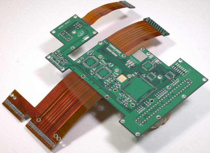
When you look at a printed circuit board (PCB), you’ll see copper traces, pads, and maybe a few shiny holes.
Those tiny holes are not just empty spaces—they’re vias, one of the most important features in multilayer PCBs.
Vias connect copper layers together and let signals, power, and heat travel through the board.
This guide explains PCB vias: what they are, the main types, sizing, best practices for tenting or filling, and reliability tips.
What Is a PCB Via?
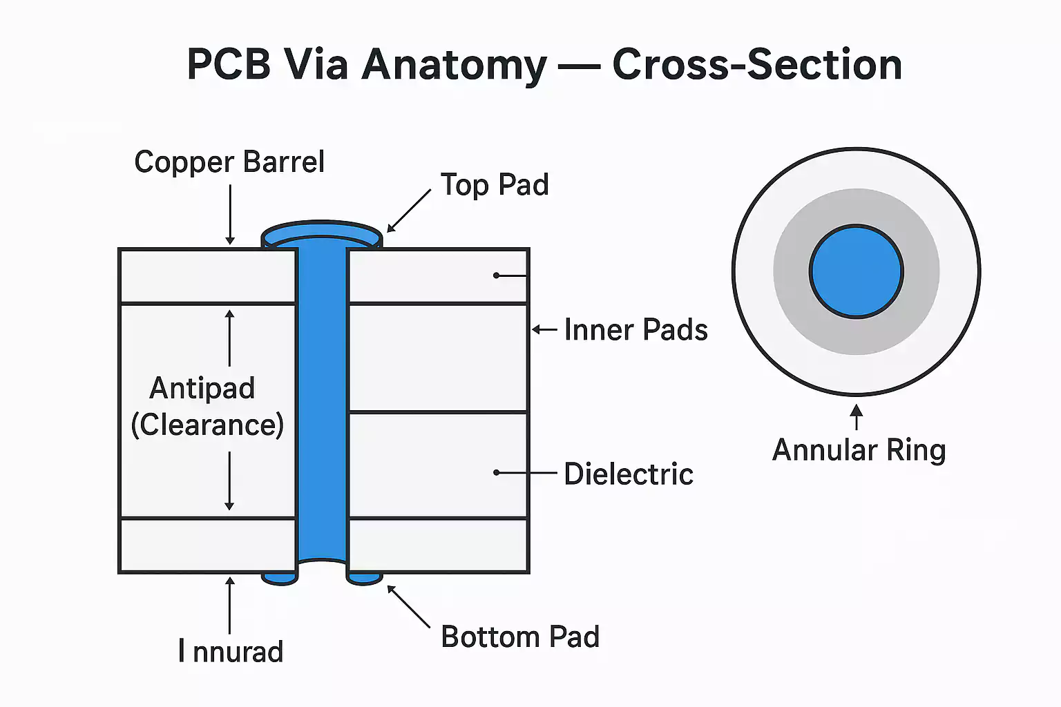
A via is a plated hole that connects copper layers in a PCB.
Each via has three parts:
- Barrel – the plated copper wall inside the hole
- Pads – copper rings on the layers, the via touches
- Antipad – the clearance area on layers where the via should not connect
A via carries electrical signals vertically between layers, just like a tiny metal tube.
Via vs. PTH: Both are types of drilled-and-plated holes on PCBs; however, their roles differ.
- PTH (Plated Through Hole) is for component leads or connectors.
- Via is only for interconnections between copper layers—no parts are inserted.
Main Types of PCB Vias
Vias come in several types, depending on where they start and end and how they’re made.
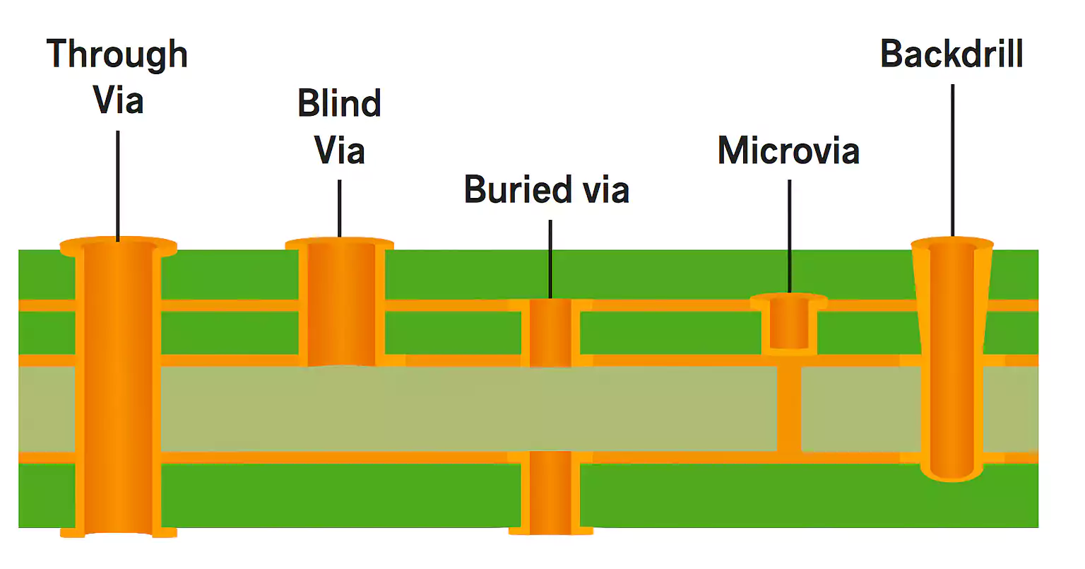
1. Through-Hole Via
This is the most common way.
It runs the entire length of the board—from top to bottom—and connects all layers.
Pros: simple, low-cost, and strong.
Cons: takes up routing space and can cause unwanted parasitic effects at high frequencies.
2. Blind Via
A blind via connects an outer layer to one or more inner layers but does not go all the way through.
They are used in HDI and BGA designs where space is tight.
Blind vias reduce routing congestion and signal length, but they require additional lamination cycles, which increase cost.
3. Buried Via
A buried via connects inner layers only—completely invisible from the surface.
They save surface space but add complexity because inner layers must be laminated before the rest of the stack-up.
4. Microvia
A microvia is a laser-drilled hole, usually less than 150 µm (≈6 mil) in diameter.
They are essential for HDI boards and stacked or staggered layer connections.
Microvias are short and have a low aspect ratio (≈0.75:1), which improves reliability.
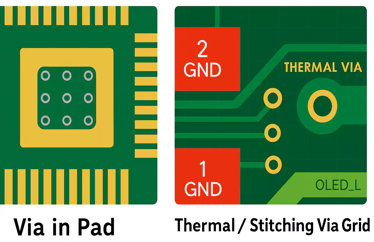
5. Via-in-Pad (VIP) / VIPPO
A via-in-pad is placed directly under a BGA pad or other fine-pitch component.
The via is filled and capped with copper, so the pad stays flat for soldering.
It saves space and improves thermal performance but requires precise filling and plating.
6. Thermal and Stitching Vias
Thermal vias help move heat from hot components to copper planes or heatsinks.
Stitching vias connects ground or power planes to reduce EMI and maintain shielding.
You’ll often see them in rows around RF sections or board edges.
7. Backdrilled Vias
A backdrill via removes the unused stub of a through-hole to improve signal integrity in high-speed designs.
This step reduces reflections on fast differential pairs and improves eye diagrams.
Size, Annular Ring & Aspect Ratio
1. Aspect Ratio (AR)
Aspect ratio is the ratio of board thickness to drilled hole diameter.
For example, a 1.6 mm-thick PCB with a 0.2 mm-diameter drilled hole has an AR of 8:1.
Higher aspect ratios are harder to plate and more likely to fail under thermal stress.
Typical limits:
- Standard through-holes: up to 10:1
- Microvias: about 0.75:1
- Reliable range: 6–8:1 for most FR-4 boards
2. Annular Ring
The annular ring is the copper area around a via hole on each pad.
A strong ring ensures a good electrical connection even with small drill misalignment.
If the drill wanders too much, the pad can “break out,” creating open circuits.
Manufacturers usually recommend a minimum ring width of 4–6 mil for standard vias.
3. Practical Size Guidelines
For common 1.6 mm boards:
- Finished hole size: 0.2–0.3 mm (8–12 mil)
- Pad diameter: hole + 10–14 mil
- Minimum spacing between vias: 0.25 mm (10 mil)
PCB Via Tenting: To Cover or Not to Cover
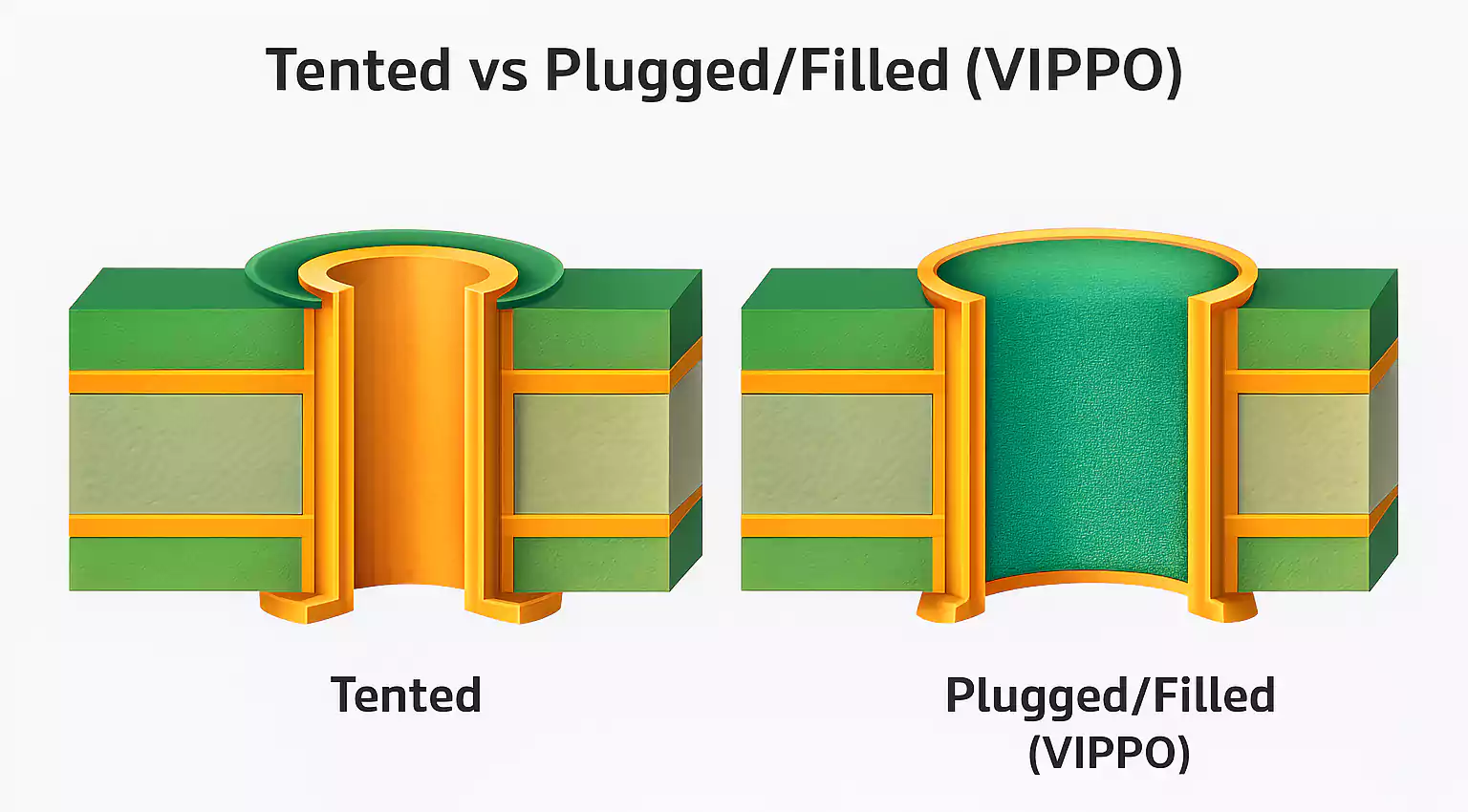
1. Common Covering Styles
- Tented: the via is completely covered by solder mask.
- Untented: the via opening remains exposed
- Plugged/Filled: via hole filled with resin or paste
- Capped: via filled and plated over with copper (used for VIP/VIPPO)
2. When to Use Tenting
Tenting keeps solder paste or contaminants from entering the hole.
It also protects the copper barrel from oxidation.
However, tenting only works well on small vias (≤12 mil finished hole)—large holes can break the mask and trap flux.
Use tented vias near fine-pitch SMT pads or BGA footprints.
For large vias or high-heat areas, plugging or filling is safer.
3. Example
- Good tenting: small signal vias under BGA chips
- Avoid tenting: power vias > 0.3 mm or test points that require probe access.
Blind Via PCB: HDI Design Essentials
Blind vias are a key part of High-Density Interconnect (HDI) boards.
They help escape BGA pads without taking extra layers.
Tips for using blind vias:
- Start and end on clearly defined layers (e.g., L1–L2, L3–L4)
- Avoid stacking more than two blind or buried vias—each stack adds lamination cost and misalignment risk.
- Keep blind vias short and low in aspect ratio (≤1:1 recommended)
Signal and Thermal Design: Treat Vias Like Components
1. Signal Integrity
- Every via adds a small parasitic inductance and capacitance. In high-speed designs, these can distort signals or cause reflections.
- Use fewer vias on critical traces, shorten via stubs, and use backdrilling when necessary.
- For differential pairs, make both vias symmetrical in length and position.
2. Thermal Management
Hot chips, power regulators, and LEDs generate heat.
You can use a grid of thermal vias to transfer heat to large copper areas or heatsinks.
For example, an array of 0.3 mm vias at a 1 mm pitch under a power pad helps evenly spread heat.
3. Ground and Shielding
Stitching vias creates a low-impedance path between ground planes.
A ring of vias spaced 1–2 mm apart around the board edge improves EMI shielding and reduces noise leakage.
Manufacturing and Testing
1. Registration Accuracy
Registration means how well each drilled hole aligns with its pad across layers.
Modern laser drills can achieve ±2–3 mil accuracy, but thick boards or stacked microvias are more sensitive to misregistration.
Poor registration can cause thin annular rings or even open circuits.
2. Testing and Inspection
Manufacturers test vias using:
- AOI (Automated Optical Inspection) – checks pad alignment and mask coverage
- Flying probe testing – measures continuity between layers.
- X-ray inspection – used for buried or via-in-pad connections under BGAs
- Microsection analysis – cuts the PCB to inspect plating thickness and voids.
Thermal cycling and stress tests confirm long-term reliability, especially for boards used in automotive or aerospace applications.
Quick Via Selection Guide
Here’s an easy way to decide what kind of via to use:
Step 1: Define the function
- Routing between layers → Through or Blind via
- Space-limited BGA → Microvia or VIPPO
- Heat removal → Thermal via array
- Shielding → Stitching vias
Step 2: Match process limits
- Check the board thickness and the manufacturer’s aspect ratio limit.
- Choose drilled or laser vias accordingly.
Step 3: Consider the environment
- Clean, indoor electronics → open or untented vias are fine.
- Dusty or humid environment → tented or filled vias for protection.
FAQ
What is a via on a PCB?
A via is a plated hole that connects copper layers in a printed circuit board.
What does “via” stand for in PCB?
“Via” comes from Latin and simply means “way” or “path”—it’s the path signals take between layers.
What is the difference between a via and a PTH?
A via is for layer-to-layer interconnection only, while a PTH is used to insert and solder component leads
How do you test vias?
Fabricators use flying-probe or X-ray inspection, and sometimes microsection analysis, to check plating quality and continuity.
What is an annular ring?
It’s the copper area around the via hole on a pad.
A ring that's too small can lead to a breakout or open circuits.
How do you pronounce “via”?
Both /ˈviːə/ (“vee-uh”) and /ˈvaɪə/ (“vye-uh”) are acceptable in the electronics industry.
What are via rivets?
They’re small metal eyelets used for manual repair or reinforcement of broken vias—rare in modern manufacturing.
Conclusion
PCB vias control how signals, power, and heat move within your board.
Choosing the right via type and size improves PCB performance, reduces costs, and extends PCB longevity.
Keep your aspect ratio reasonable, use tented or filled vias where needed, and always confirm design limits with your PCB manufacturer.
