When you design or order a printed circuit board, “PCB thickness” is one of those numbers you’ll see on every quote form. It might look like a small detail—but that thickness affects everything from mechanical strength and impedance to how your board fits inside an enclosure.
This guide explains standard PCB thicknesses, tolerance rules, and a simple 3-step method to pick the right option for your next project.
TL;DR: The Quick Answer
- The most common standard PCB thickness is 1.6 mm (≈ 0.062 inch).
- Other typical sizes include 0.8 mm, 1.0 mm, 1.2 mm, 2.0 mm, and 2.36 mm.
- Most manufacturers can produce PCBs from 0.2 mm up to about 3.2 mm, with ±10 % tolerance.
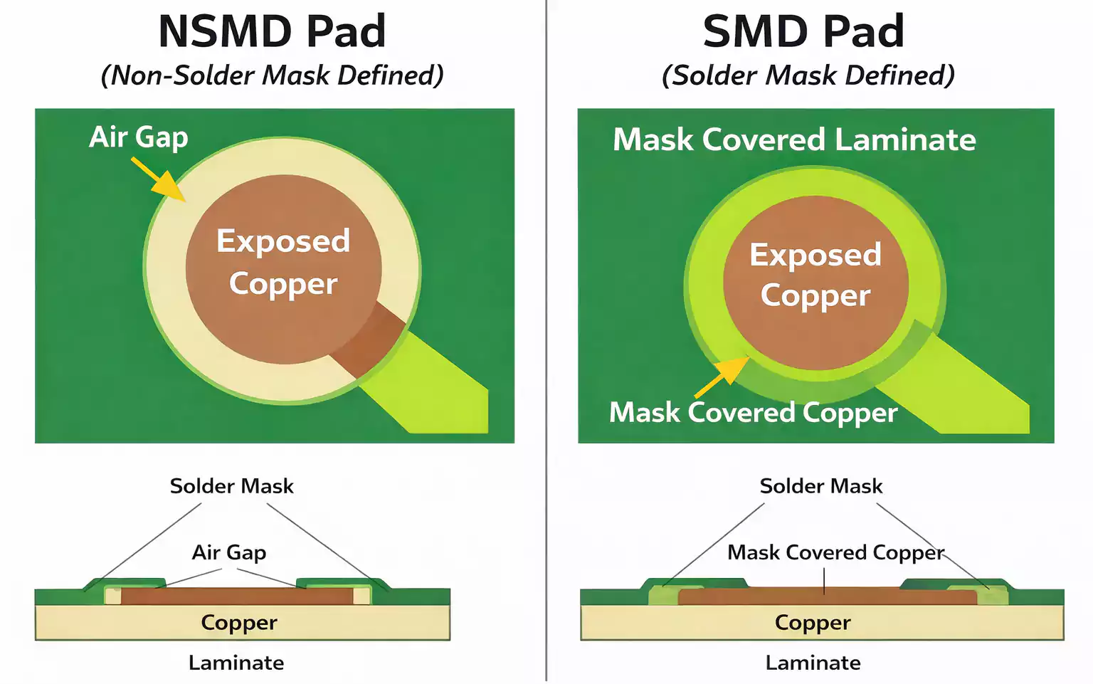
What “PCB Thickness” Really Means
PCB thickness refers to the total finished thickness of the board—including all copper layers, dielectric materials, and outer coatings such as solder mask or surface finish.
Manufacturers usually list the value in millimetres (mm), inches (in), or mils (1 mil = 0.001 inch ≈ 0.0254 mm).
A common FR-4 board that’s 1.6 mm thick equals about 62 mils.
The total thickness is composed of the core laminate, prepreg (bonding) layers, and copper plating.
Since copper thickness is often expressed in ounces per square foot, remember this rule of thumb:
1 oz copper ≈ 35 µm ≈ 1.37 mils per layer
Thicker copper adds both mechanical stiffness and total PCB thickness.
Standard PCB Thickness Values
The electronics industry settled on 1.57 mm (1/16 inch) as a de facto standard decades ago because it fit easily into connectors, enclosures, and mounting hardware. Most modern boards still follow this convention.
However, there’s no single “official” number. Here are the most common options you’ll find in manufacturing catalogues:
| 0.2 – 0.4 mm | 0.008 – 0.016 in | Ultra-thin, flex/rigid-flex support cores |
| 0.6 mm | 0.024 in | Space-saving modules |
| 0.8 mm | 0.031 in | Thin consumer boards, wearables |
| 1.0 – 1.2 mm | 0.039 – 0.047 in | Compact multilayer devices |
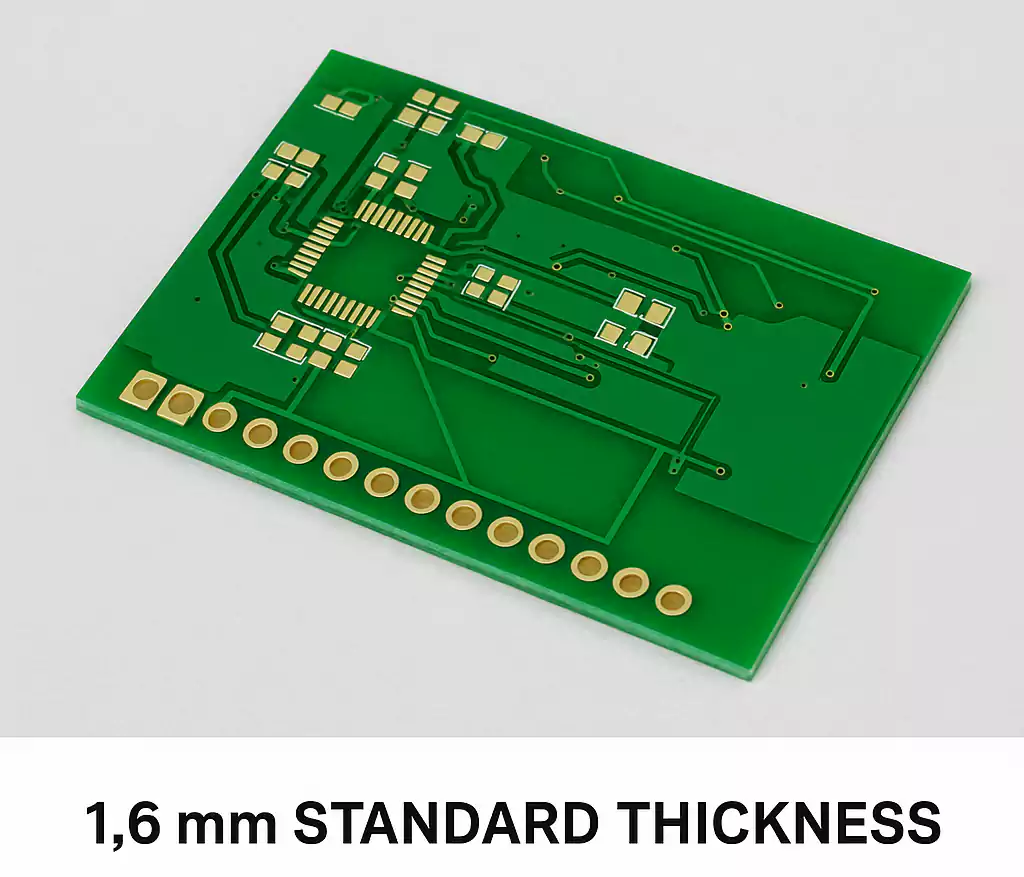
| 1.6 mm | 0.062 in | Industry standard, 2–6 layer boards |
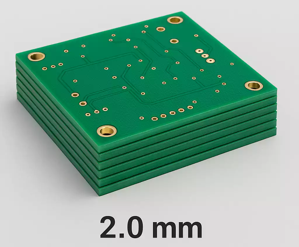
| 2.0 mm | 0.079 in | Power boards, connectors, or large panels |
| 2.36 – 3.2 mm | 0.093 – 0.125 in | Heavy-duty or mechanical strength designs |
Most PCB fabricators allow a tolerance of ±10% for boards ≥ 1.0 mm thick and ±0.1 mm for thinner boards.
PCB Thickness Chart: Metric / Inch / Mil
| 0.2 | 0.008 | 8 | flex reinforcement |
| 0.4 | 0.016 | 16 | ultra-thin sensors |
| 0.6 | 0.024 | 24 | IoT modules |
| 0.8 | 0.031 | 31 | wearables, drones |
| 1.0 | 0.039 | 39 | compact 4-layer |
| 1.2 | 0.047 | 47 | small devices |
| 1.6 | 0.062 | 62 | general 2–6 layer boards |
| 2.0 | 0.079 | 79 | power or industrial boards |
| 2.36 | 0.093 | 93 | connectors, heavy loads |
| 3.2 | 0.125 | 125 | mechanical panels |
Many plastic housings, keyboard frames, and card-edge connectors are designed for PCB slots measuring approximately 1.6 mm.
Why Thickness Matters
1. Mechanical Strength
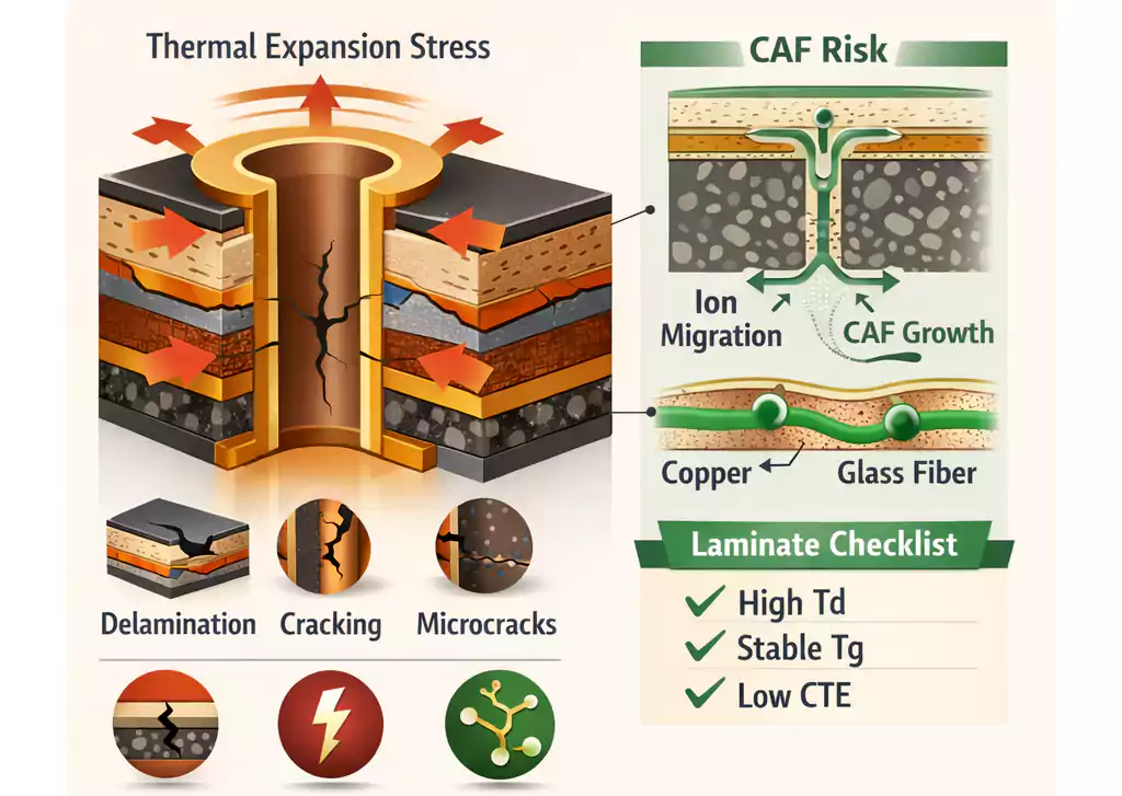
Thicker PCBs resist bending and warping during assembly or operation.
Boards thinner than 1 mm may flex under connector stress or reflow temperature changes. If your board is large or has heavy components, go thicker (1.6–2.0 mm).
2. Electrical & Signal Integrity
Signal impedance depends on dielectric height and trace width.
Changing the board thickness alters the dielectric distance between copper layers, which can shift your impedance target (for example, 50 Ω microstrip).
High-speed designs may need precise control over stack-up and thickness.
3. Thermal and Manufacturing Aspects
A thicker board spreads heat better but can trap stress during lamination.
During plating and surface finishing, thickness may increase slightly—usually a positive tolerance.
Manufacturers must balance the drill aspect ratio (hole depth to diameter) and layer symmetry; a board that is too thick or a board with tiny vias may fail plating tests.
The 3-Step Method to Choose the Right PCB Thickness
Step 1 – Start from Your Application
| Ultra-compact wearables | 0.6 – 1.0 mm |
| General electronics, IoT, consumer | 1.6 mm (default) |
| Industrial / power / connectors | 2.0 – 2.36 mm |
| Heavy mechanical load or backplane | ≥ 2.36 mm |

Step 2 – Refine by Electrical & Layer Stack
For multilayer designs, thickness is the sum of the core, prepreg, and copper plating.
A 4-layer PCB can remain at 1.6 mm by simply changing the inner dielectric thickness.
If you need impedance-controlled traces (50 Ω or 90 Ω differential), adjust the dielectric spacing rather than the total thickness first.
Copper thickness also matters:
- 1 oz = 35 µm (standard)
- 2 oz = 70 µm (power)
- 3 oz + = heavy copper for thermal/amp capacity
Thicker copper may require thicker prepreg to maintain proper spacing, raising the overall board height.
Step 3 – Verify Manufacturing Limits & Tolerance
Every PCB house publishes a capability table—check these before finalising:
| Finished thickness range | 0.2 – 3.2 mm |
| Tolerance ≥ 1.0 mm | ±10 % |
| Tolerance < 1.0 mm | ±0.1 mm |
| Aspect ratio (hole depth / diameter) | ≤ 8 : 1 |
| Max copper weight | 6 oz |
Recommended Thickness by Layer Count
| 2-Layer | 1.6 mm default (range 0.8–2.0 mm) | Most common for prototypes and hobby boards. Thinner = compact, thicker = stronger. |
| 4-Layer | 1.2 – 1.6 mm | Adjust dielectric to control impedance. |
| 6–8 Layer | 1.6 – 2.0 mm | Keep stack-up symmetrical to reduce warpage. |
| 10 Layer + | 2.0 mm + | Needed for complex HDI, power, or backplanes. |
Symmetry and copper balance are key. Avoid “copper-heavy” one-sided stacks that can warp during lamination.
Tolerance and Minimum Thickness Explained
Tolerance is the acceptable variation between your design value and the actual finished board.
Because plating and coatings add small increments, the final board often ends up slightly thicker than the design spec.
Typical values:
- ≥ 1.0 mm: ±10 %
- < 1.0 mm: ±0.1 mm
Minimum thickness for standard rigid FR-4 PCBs is around 0.2–0.4 mm.
Anything thinner usually moves into flex or rigid-flex territory, requiring special materials and reinforcement stiffeners.
FAQ
1) What is the standard PCB thickness (mm / inch)?
The global standard is 1.6 mm (≈ 0.062 in), but many manufacturers offer 0.8–2.36 mm options.
2) What is the standard thickness for a 2-layer PCB?
Usually 1.6 mm. Thin consumer boards may use 0.8–1.2 mm; large or connector-loaded boards may use 2.0 mm.
3) What’s the normal tolerance for PCB thickness?
Typically ±10 % for boards ≥ 1 mm thick and ±0.1 mm for thinner boards. Always confirm with your supplier’s specs.
4) What is the minimum PCB thickness?
Rigid PCBs can be as thin as 0.2 – 0.4 mm, but handling becomes delicate. Below that, switch to flexible or rigid-flex materials.
5) How is trace (copper) thickness related to board thickness?
Copper thickness is measured in ounces (oz).
1 oz ≈ 35 µm ≈ 1.37 mils.
It contributes slightly to total thickness and strongly affects current capacity and thermal behavior.
6) Is there a PCB thickness calculator?
Yes. Many board houses provide online calculators and stack-up viewers. They show how copper weight and dielectric height combine to reach your desired impedance.
Conclusion
Choosing the right PCB thickness isn’t complicated once you know what drives the decision.
Start from your mechanical needs, verify electrical and layer requirements, and confirm manufacturing tolerance with your board house.
If you’re unsure, 1.6 mm remains the safest and most compatible option across connectors, assemblies, and enclosures.