


When you design or build a printed circuit board (PCB), testing is not an optional step—it’s the final checkpoint that decides whether your board will actually work. A single open trace or shorted pad can stop the entire system.
This guide breaks down what PCB testing really means, the main methods used in the industry, how to choose between them, and what design choices make testing easier and cheaper.
What Is PCB Testing and Why Does It Matter
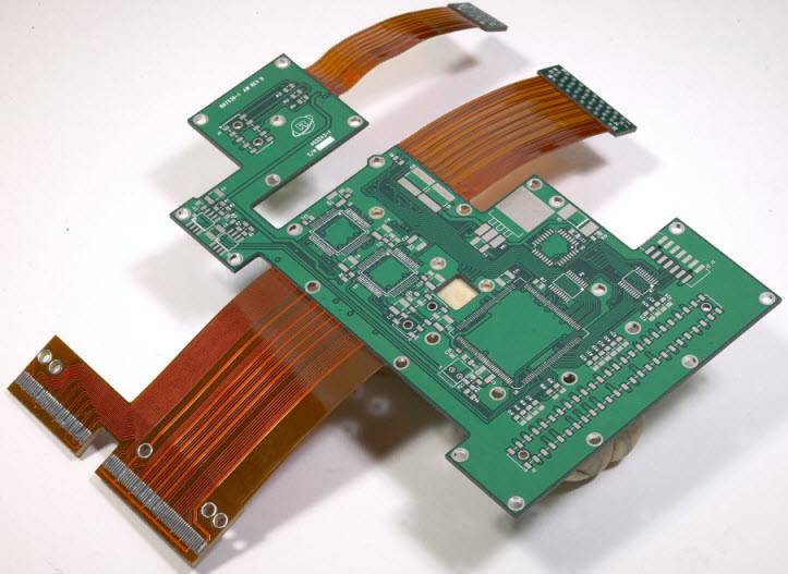
PCB testing is the process of verifying that a circuit board has been correctly manufactured and assembled. It checks that every trace, component, and solder joint performs as intended.
In modern production, testing protects yield, reduces field failures, and ensures compliance with quality requirements.

Testing typically happens in two phases:
- Bare board test – verifies copper connectivity before assembly.
- Assembled board test – confirms that components are placed, soldered, and functional.
The key techniques you’ll hear about include ICT (In-Circuit Test), FPT (Flying Probe Test), AOI (Automated Optical Inspection), AXI (X-ray), Burn-in, and FCT (Functional Test).
Each plays a unique role in catching different types of faults.
Main PCB Testing Methods and When to Use Them
Different testing methods target different problems. Understanding how each one works will help you choose the right mix for your product.
In-Circuit Test (ICT)
Principle: ICT uses a bed-of-nails fixture with hundreds of spring-loaded probes that contact test points on the PCB. The system applies voltage and measures resistance, capacitance, and signal paths.
Advantages:
- Very fast test cycle (seconds per board)
- Detects opens, shorts, wrong components, and missing parts.
- Excellent coverage and repeatability
Limitations:
- High upfront cost for fixture and programming
- Limited flexibility after design changes
Best for: High-volume, stable products where speed and coverage matter.
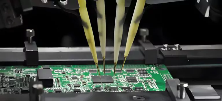
Flying Probe Test (FPT)
Principle: Instead of a fixed fixture, flying probe testers use a few movable needles that “fly” across the board to contact test pads one by one. It measures continuity, resistance, capacitance, and sometimes diode or transistor behaviour.
Advantages:
- No fixture—fast setup and low initial cost
- Works well for prototypes and small batches
- Easy to update when the design changes
Limitations:
- Slower test cycle (minutes per board)
- Coverage may drop if there are no accessible test pads.
Best for: Prototyping, small-batch runs, or high-density boards that can’t fit many test points.
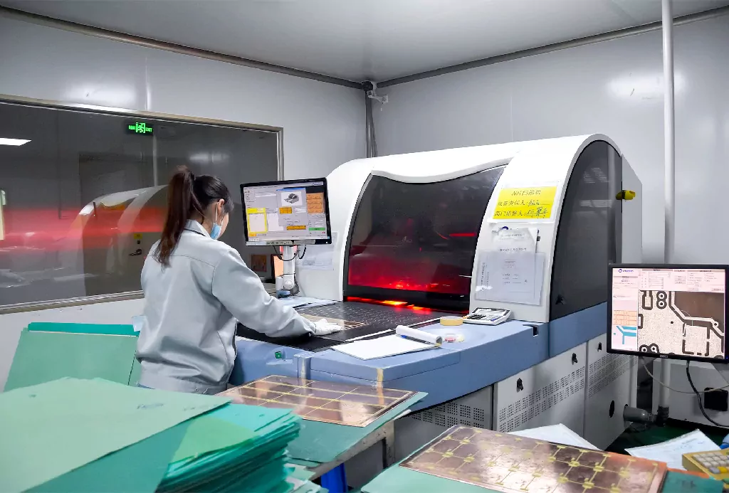
AOI and AXI (Optical and X-ray Inspection)
AOI uses high-resolution cameras and image processing to detect missing components, polarity errors, bridges, or solder voids.
AXI uses 3D X-ray to see inside BGA and hidden solder joints that cameras cannot reach.
Advantages:
- Non-contact and non-powered testing
- Excellent at catching solder defects early
- Can be automated in-line for high throughput
Limitations:
- Cannot detect electrical issues
- False positives may require manual review.
Best for: All production lines—AOI/AXI should run before electrical testing to avoid wasting time on bad solder joints.
Burn-In Test
Principle: Burn-in testing runs the board under elevated temperature, voltage, or load for hours or days to expose early failures.
Advantages:
- Screens out “infant mortality” failures
- Improves long-term reliability data
Limitations:
- Time-consuming and may slightly shorten lifespan
- Adds stress and energy cost
Best for: Aerospace, medical, automotive, and other high-reliability products.
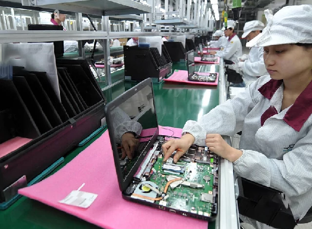
Functional Test (FCT)
Principle: FCT verifies that the complete PCB or assembled product performs its real function. The board is powered on, connected to peripherals, and tested in a controlled environment.
Typical checks:
- Power-up sequence and self-test
- Communication ports (USB, Ethernet, CAN, UART)
- Voltage, current, or frequency limits
- Sensor feedback and logic output
Advantages:
- Simulates real-world operation
- Detects system-level issues missed by ICT or AOI
Limitations:
- Requires a working firmware or test program
- Test time and fixture cost are higher.
Best for: Final verification before shipment or integration into larger assemblies.
Other Specialised Tests
Depending on the product and customer requirements, you may also perform:
- Impedance and TDR tests for high-speed signals
- Solderability and contamination tests for surface quality
- HiPot (isolation) and peel strength for safety and adhesion
Quick Comparison Table
| ICT | Yes | High | Very fast | High | Mass production |
| Flying Probe | Yes | Medium | Slow | Low | Prototype, small batch |
| AOI/AXI | No | Visual | Fast | Medium | Solder inspection |
| Burn-in | Yes | Reliability | Very slow | Medium | Critical systems |
| FCT | Yes | System-level | Moderate | Medium-High | Final validation |
How to Choose the Right Testing Strategy
There’s no single “best” method—each stage of your project needs a different balance between speed, coverage, and cost.
Step 1: Identify your stage
- Prototype / engineering sample: Flying Probe + AOI
- Pre-production: AOI + limited ICT or FCT
- Mass production: ICT + AOI/AXI + FCT
Step 2: Evaluate board design
- Dense BGA or fine-pitch parts → Add AXI
- Few test pads or frequent revisions → Flying Probe
- Simple through-hole design → ICT is efficient.
Step 3: Consider risk and reliability
- Safety-critical or high warranty cost → Add Burn-in + FCT.
- Consumer electronics with short life cycle → AOI + ICT may be enough.
Choosing the right mix saves both time and rework later.
DFT (Design for Testability): Build It Right from the Start
Testing efficiency starts in the PCB layout stage. A few small choices can make or break your future test plan.
Test Point Planning
- Place dedicated test pads for power, ground, and key nets.
- Keep probe access clear—avoid tall components or shielding nearby.
- Maintain a spacing of 50–75 mil for bed-of-nails probes.
- Distribute ground reference pads to reduce noise.
Data and File Preparation
- Provide BOM, netlist, and manufacturing files (ODB++ or IPC-2581).
- They allow automated test program generation for both ICT and FPT.
Layout Tips
- Avoid dropping test points on large copper pours.
- Keep signal and ground paths short for stable readings.
- Mark polarity clearly for optical systems.
Typical Workflow
AOI → ICT or FPT → AXI (if needed) → FCT.
This layered approach catches defects early, reduces debug loops, and improves final yield.
Functional Testing (FCT) in Action
Functional testing is often the final gate before shipping. It ensures the board behaves as a complete product, not just a connected network.
Basic Setup
A typical FCT station includes:
- A power supply or electronic load
- Interface cables and connectors
- Measurement instruments (DMM, oscilloscope)
- A test fixture or jig to position the board
- Software or firmware that runs automated sequences
Test Flow
- Power on and safety checks
- Firmware download or boot sequence
- Interface communication (USB, CAN, Wi-Fi, etc.)
- Load and stress tests
- Pass/fail report and barcode traceability.
Common Challenges
- Longer test time and need for consistent firmware versions.
- Risk of over-voltage or short circuit (use current limiters)
- Fixture wear or alignment errors over time
Even with these challenges, FCT remains critical. It validates the “real world” performance that electrical and optical tests can’t fully prove.
Common Equipment, Software & Test Kits
On the Production Line
- ICT stations with pneumatic fixtures
- Flying probe testers (single or double-sided)
- AOI / AXI machines
- Burn-in ovens and racks
- FCT benches with programmable supplies and measurement tools
Software
- Test-program generators for ICT/FPT
- Probe path optimisation
- Statistical Process Control (SPC) dashboards for yield tracking.
- Data loggers for traceability
Basic Lab or R&D Test Kit
For small teams or engineers validating prototypes:
- Adjustable DC power supply
- Electronic load or resistor bank
- Multimeter and oscilloscope
- Jumper wires, clips, and ESD protection
- Small test jig or socket adapter
These simple tools can cover 80 % of troubleshooting needs before formal production testing.
Frequently Asked Questions (FAQ)
1. What’s the difference between PCB testing and inspection?
Inspection (like AOI or AXI) checks visual or structural defects. Testing (ICT, FPT, FCT) measures electrical and functional behaviour. They complement each other.
2. Will flying probe testing damage my board?
No. Modern probes apply very light pressure—just enough for contact. It’s a non-destructive, safe process.
3. When is ICT worth the investment?
If you expect thousands of identical boards per month, ICT pays off quickly thanks to its speed and repeatability.
4. Do I always need a functional test?
For consumer or low-risk designs, AOI + ICT may be enough. But for complex or safety-critical products, FCT is the only way to confirm true performance.
5. Does burn-in reduce lifespan?
Extended stress can slightly age components, but proper burn-in (controlled time and temperature) exposes weak parts without harming healthy ones.
Final Thoughts
Choosing the right PCB testing method isn’t always easy. There are many options—each with different strengths, trade-offs, and ideal use cases.
Whether you’re prototyping with a desktop PCB printer or scaling up to production, the right testing strategy helps you avoid delays, reduce defects, and protect product quality.
