

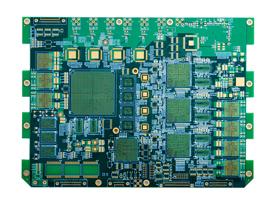
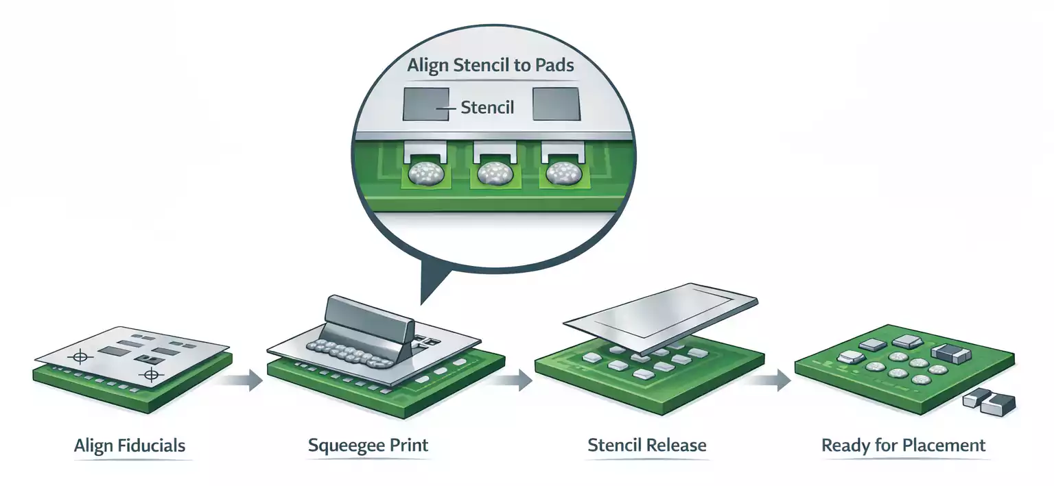
In surface mount PCB assembly, precision starts before components ever touch the board.
The PCB stencil plays a key role in this process — it controls how much solder paste is printed on each pad and directly affects solder joint quality.
This guide explains what a PCB stencil is, how it’s made, key design parameters like thickness and aperture ratio, and how to avoid common printing defects.
What Is a PCB Stencil?
A PCB stencil is a thin sheet of stainless steel or nickel with laser-cut openings that match the pads on a circuit board.
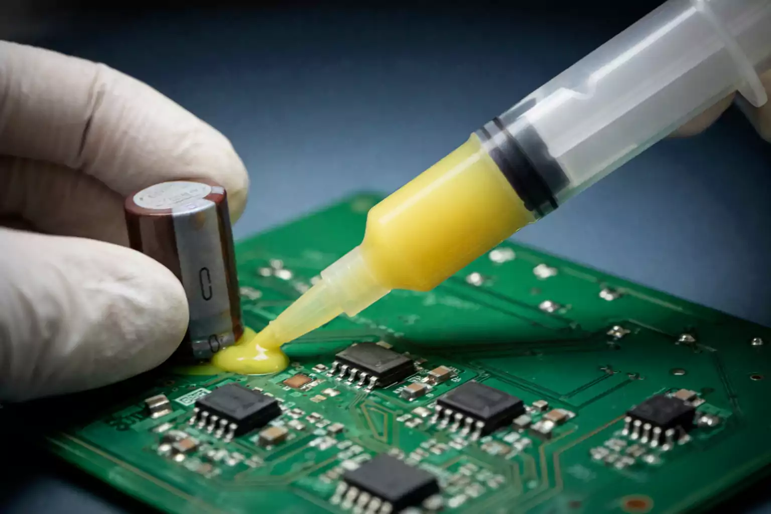
During surface-mount assembly, solder paste is spread across the stencil using a metal squeegee. The paste passes through the openings and deposits onto the PCB pads underneath.
When the stencil is lifted, small, uniform deposits remain on each pad — ready for component placement and reflow soldering.
The stencil ensures consistent solder paste application, resulting in reliable joints during reflow.
Structure and Common Types
A stencil usually consists of:
- Frame or frameless design
- Metal foil (steel or nickel)
- Mesh and adhesive (for framed stencils)
The main stencil categories include:
| Framed (with mesh) | Stainless steel foil mounted on an aluminum frame. | High-volume production, repeated use. |
| Frameless | Loose foil held by a tension system. | Prototyping and small batches. |
| Laser-cut | High accuracy, smooth sidewalls, industry standard. | Most SMT production lines. |
| Chemical etched | Low cost, rougher edges. | Low-precision or large-pitch designs. |
| Electroformed (nickel) | Best paste release for fine-pitch parts. | Micro-BGA, 0201, 01005 components. |
Each type balances cost, precision, and durability.
Laser-cut and electroformed stencils are preferred for fine-pitch SMT and high-yield production.
Manufacturing Methods
There are three main manufacturing technologies:
- Laser Cutting:
Uses high-precision laser beams to create openings. It offers smooth walls and tight tolerance, making it the industry’s default method. - Chemical Etching:
Involves photoresist and acid to etch openings from both sides. Cheaper but produces tapered edges, which can trap paste. - Electroforming:
Builds a nickel stencil layer by layer through electroplating. Extremely smooth and accurate, ideal for ultra-fine components, but more expensive and slower to produce.
Key Design Parameters
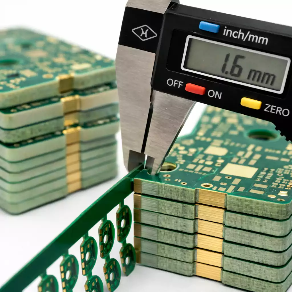
1. Stencil Thickness
Stencil thickness defines how much paste volume is printed.
Too thick — you risk solder bridging.
Too thin — insufficient solder causes opens or tombstones.
Typical thickness ranges:
| 01005 / 0201 passive | 0.10 mm (4 mil) |
| QFN / Fine-pitch BGA | 0.12 mm (4.7 mil) |
| Standard SMT | 0.13–0.15 mm (5–6 mil) |
| Large pitch / connectors | 0.18–0.20 mm (7–8 mil) |
2. Aperture Design and Ratio Rules
The stencil aperture determines how easily solder paste releases during printing.

Two ratios help designers optimize openings:
- Aspect Ratio = Aperture Width / Stencil Thickness
→ Recommended ≥ 1.5 for reliable paste release. - Area Ratio = (Aperture Area) / (Aperture Wall Area)
→ Recommended ≥ 0.66 for most solder pastes.
If ratios fall below these limits, solder may stick in the stencil rather than transfer to the pads.
This leads to insufficient solder or open joints during reflow.
Aperture shapes can be fine-tuned:
- Rounded corners improve paste flow.
- Window or segmented openings help control volume on thermal pads (like QFN).
- Home plate shapes reduce bridging on small pads.
Printing and Alignment Best Practices
Even a perfect stencil can fail without a proper printing setup.
Key variables include:
- Squeegee Pressure & Speed:
Enough pressure to wipe cleanly, but not too much to squeeze paste under the stencil.
A moderate speed (20–40 mm/s) usually works well. - Snap-off (Separation) Distance:
The gap between the stencil and the PCB during printing. Modern printers often use 0-gap (contact printing) with controlled separation. - Alignment (Fiducials):
Always align the stencil using fiducial marks on both the stencil and the PCB for high accuracy. Misalignment causes offset solder deposits. - Cleaning Frequency:
Regular dry or wet wipes every few prints prevent clogging and paste smearing. Vacuum cleaning systems help with fine-pitch jobs.
These process controls ensure consistent paste transfer and reduce defects before placement.
Common Defects and How to Prevent Them
| Solder bridging | Too thick stencil, excessive paste, poor aperture shape | Use thinner stencil or windowed openings |
| Insufficient solder | Low area/aspect ratio, blocked apertures, dry paste | Redesign openings, clean stencil, adjust viscosity |
| Tombstoning | Unequal paste volume on pads | Balance aperture size for small components |
| Solder balling | Excess paste, fast reflow ramp | Control print volume, optimize reflow profile |
| Offset / Smearing | Misalignment or poor cleaning | Realign, clean stencil frequently |
| Voids (bubbles) | Paste trapped under large pads | Use windowpane design, slower separation |
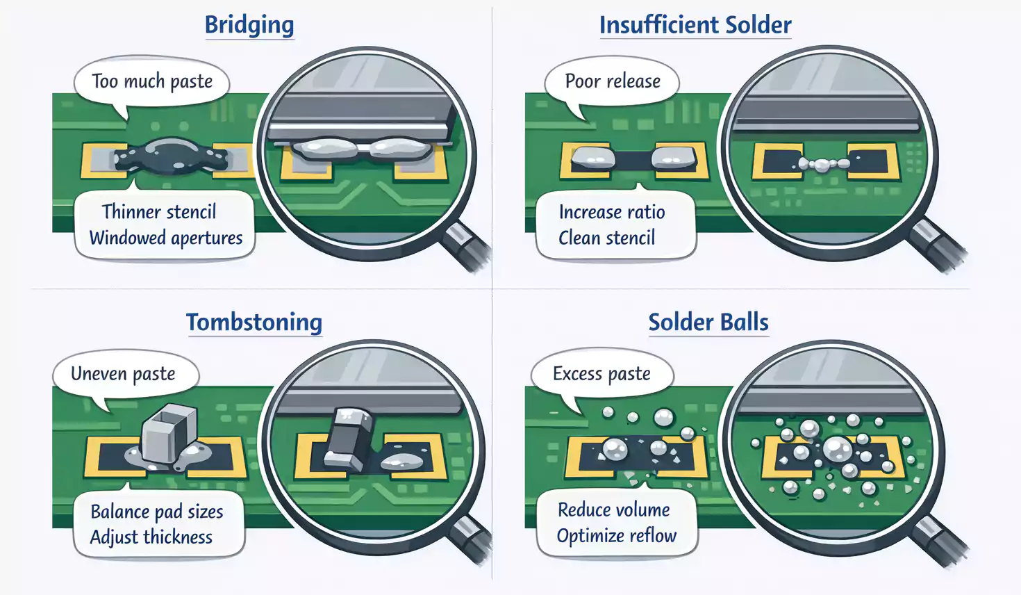
Understanding the link between defect and cause helps improve print yield and reliability.
Frequently Asked Questions
Q1: What stencil thickness should I use for fine-pitch BGA or QFN?
Usually, 0.10–0.12 mm works best. Use electroformed or laser-cut stencils for the smoothest release.
Q2: How often should I clean my stencil?
Every 5–10 prints is a safe rule. For ultra-fine pitch (<0.4 mm), clean more frequently.
Q3: Can one stencil be reused for different boards?
Only if the pad layout and board size are identical. Otherwise, alignment will fail.
Summary
A PCB stencil is a precision tool that defines the quality of every solder joint in surface mount assembly.
Choosing the right thickness, aperture ratios, and manufacturing type — combined with good printing control — ensures strong, uniform solder joints and higher production yield.
Whether you are building prototypes or mass-producing boards, understanding stencil basics is essential for any SMT process.
