


When you design a printed circuit board (PCB), the first and most important step is creating the schematic.
A clear, correct schematic ensures easy manufacturing and assembly; a confusing schematic risks failure in later steps.
This guide explains what a PCB schematic is, how to draw it correctly, and how it connects to real PCB fabrication files, such as Gerber.
What Is a PCB Schematic and Why Does It Matter?
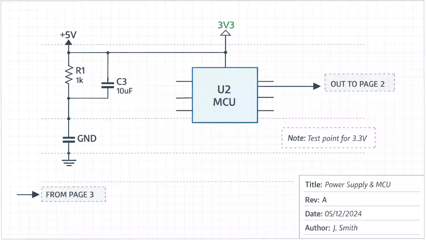
A PCB schematic is a visual representation of an electronic circuit. It shows how components such as resistors, capacitors, ICs, and connectors are connected by signals or “nets.”
Think of it as a map for your design — it doesn’t show the physical board layout yet, but it defines all electrical logic and relationships.
The schematic drives three critical outputs:
- Netlist – Defines how components are connected.
- BOM (Bill of Materials) – Lists all parts and quantities.
- Reference Designators – Labels like R1, C5, U2 that connect to layout and assembly.
Without a proper schematic, there is no PCB layout, no manufacturing, and no debugging.
PCB vs. PCBA: Know the Difference Before You Start
Many beginners mix up PCB and PCBA. Here’s the simple difference:
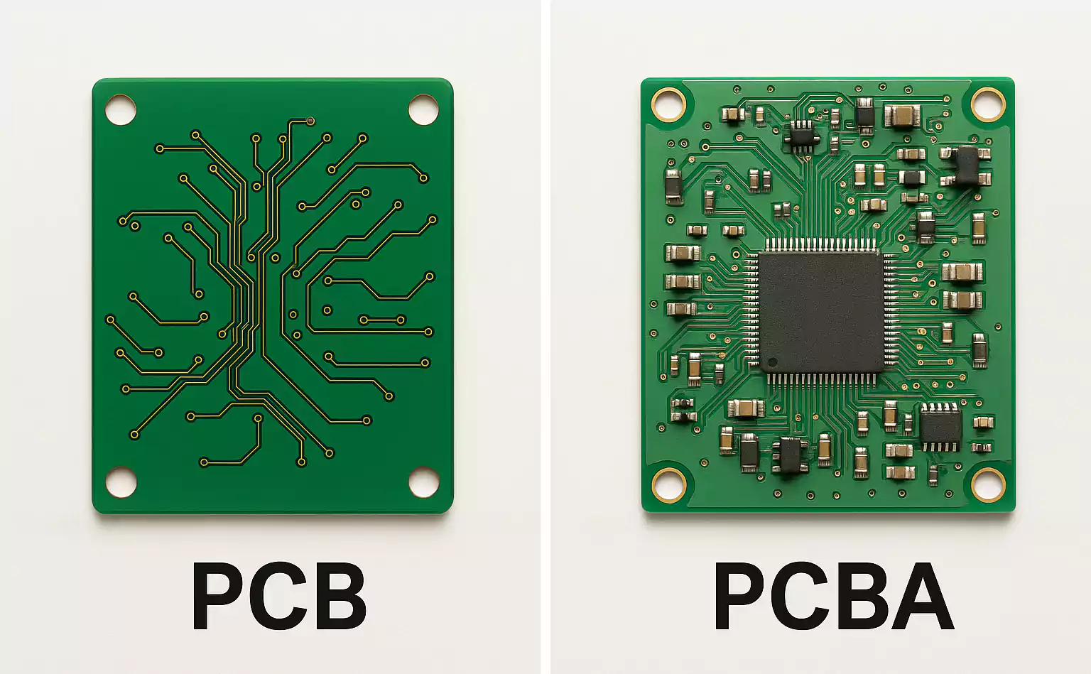
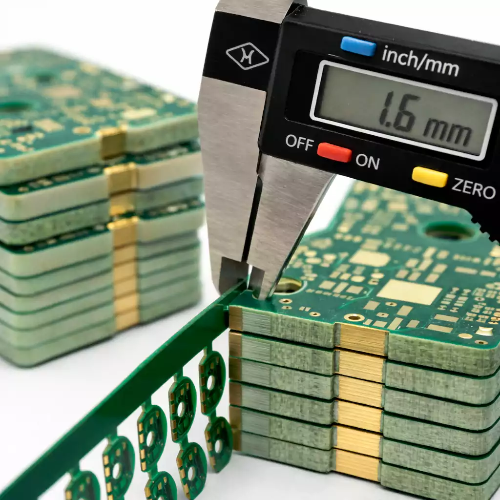
| PCB (Printed Circuit Board) | Bare copper board with no components | Gerber files, drill files, stack-up info |
| PCBA (Printed Circuit Board Assembly) | PCB with all parts soldered | BOM, Pick-and-Place file, assembly drawing |
A PCB is just the base board — copper, laminate, and housing. A PCBA is the finished product after components are soldered.
Symbols, Labels, and Naming: Keep It Clean and Consistent
A clear schematic follows simple naming rules:
- Reference Designators: Use common prefixes (R for resistor, C for capacitor, U for IC, J for connector).
- Net Names: Label important signals like “VCC_3V3” or “USB_DP.”
- Power and Ground: Always define your power symbols clearly (VCC, GND, +5V, etc.).
- Annotations: Add notes for special components or jumpers.
Consistency avoids confusion during layout and assembly.
Common EDA Tools for Drawing Schematics
You can create schematics with many EDA (Electronic Design Automation) tools. Popular choices include:
- Altium Designer – Professional, used in large companies.
- KiCad – Free and open-source, great for hobby or small business.
- OrCAD / Cadence – Common in enterprise and complex hardware.
Choose a tool that fits your team size, budget, and workflow. The most important feature is a smooth netlist and BOM export — that’s what connects the schematic to PCB layout and manufacturing.
How to Draw a PCB Schematic: Step-by-Step
1. Start with a Functional Block Diagram
Before adding parts, group the design by function—power supply, controller, sensors, interface, etc. This keeps the schematic organized from the start.
2. Choose and Add Components
Select parts that meet electrical and performance needs. Add key specs (voltage, current, tolerance) and assign actual manufacturer part numbers (MPNs).
3. Connect the Nets
Draw wires to connect component pins. Use clear net names, like “SCL,” “TX,” or “VCC_5V.” Maintain the flow from left to right or top to bottom.
4. Annotate the Design
Assign reference designators automatically (R1, R2, C1, etc.). Add text notes and page numbers to help with navigation.
5. Run ERC/DRC Checks
Use your tool’s built-in ERC (Electrical Rule Check) to find missing connections, unconnected pins, or power conflicts. This step catches 90% of typical schematic errors.
6. Generate the BOM and Netlist
Export the BOM and netlist. Check that every component has a footprint and the correct parameters before sending it to PCB layout.
By following these steps, you’ll have a schematic that’s not only functional but also production-ready.
From Schematic to PCB Layout
Once your schematic passes checks, it’s time to create the PCB layout.
The schematic sends the netlist to the layout tool, defining how each pad must connect.
At this stage, design synchronization matters:
- If you rename a component or change a connection, update the schematic first.
- Use ECO (Engineering Change Order) or synchronization tools to keep data aligned.
- Double-check footprints and orientation before routing traces. A mismatch between schematic and layout is one of the top causes of manufacturing errors.
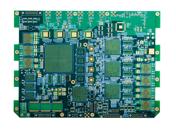
After layout, you’ll output Gerber files — these are the standard manufacturing files every PCB factory uses.
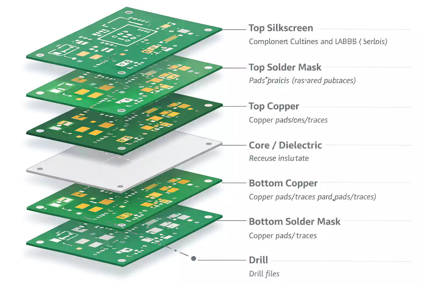
Each layer in your board (copper, solder mask, silkscreen, drill, mechanical) has its own Gerber file.
Together, they define how the physical board will be made.
How to Read a PCB Schematic (Quick Guide for Reviewers)
Even if you didn’t design the circuit, you can quickly understand it by following this order:
- Look at the title block – project name, date, and revision.
- Find the block diagram or power page first.
- Trace the main power rails and ground connections.
- Locate the main IC or controller and follow its inputs/outputs.
- Check clocks, resets, and communication lines (SPI, UART, USB, etc.).
- Review protection circuits (ESD, fuses, diodes).
- Read the connector pins and test points at the edges.
This method helps engineers, technicians, and reviewers get context fast.
Common Questions
Q: What’s the difference between a schematic diagram and a PCB layout?
A schematic shows logical connections; a layout shows physical copper routing on the board.
Q: What is a “schematic diagram of PCB”?
It’s just another way to say PCB schematic — the diagram that defines how a PCB should be wired.
Conclusion
Creating a clear, well-organized PCB schematic is the foundation of every successful electronic design.
When you follow standard naming, clean symbols, and proper ERC checks, your schematic will flow smoothly into layout and manufacturing.
If you’re looking for reliable PCB manufacturing and assembly from schematic to finished board, FastTurnPCB is here to help.
We specialize in fast, accurate PCB prototyping and full PCBA service — turning your schematic into a working product with quality you can trust.
