PCB Panelization in modern electronics now means more than simply combining boards on a single sheet.
For production engineers, a well-designed panel determines how fast a product moves through stencil printing, pick-and-place, reflow, inspection, and testing.
This guide covers the engineering of panel design: fiducials, rails, mouse bites, depaneling stress, and production survival.

From “Can Be Made” to “Easy to Build.”
Traditional articles describe panelization as a way to save material and process many PCBs at once.
That’s true, but it misses the point: in real factories, PCB Panelization is about alignment, rigidity, and handling.
A panel that is easy to align, clamp, and depanel saves minutes per cycle and prevents scrap from cracked solder joints or warped arrays.
If your boards are smaller than 50 × 50 mm or have irregular shapes, PCB Panelization is almost mandatory.
Without rails or support frames, tiny boards wobble on conveyors, smear solder paste, and mis-register during AOI.
Rails, Fiducials, and Tooling Holes — The Alignment Trio
Rails (Handling Edges)
Rails, or process edges, are the extra margins added around the PCB array to allow machines to grip and transport panels.
A width of 200-400 mil (5–10 mm) on each side usually works well.
If the board carries heavy components or connectors near the edge, go wider to avoid bending.
Fiducials
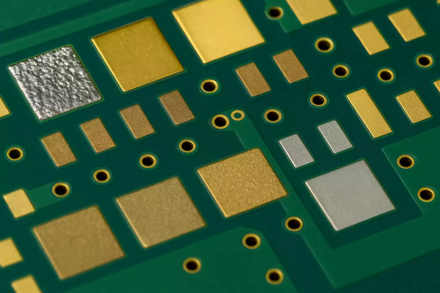
Fiducials are small, exposed copper pads that serve as optical alignment marks for pick-and-place and AOI systems.
Global fiducials are placed on the rails, while local fiducials are placed near fine-pitch components such as BGAs.
Typical diameter: 1 – 3 mm (≈40 – 120 mil), with a clear solder-mask opening around each pad.
Use three fiducials in an asymmetric triangle so the machine can detect rotation as well as position.
Tooling Holes
Tooling holes are mechanical reference points for stencils, reflow pallets, and ICT or FCT fixtures.
A 3 mm (≈118 mil) hole size with two diagonal holes on opposite corners is a proven standard.
Always keep copper and components at least 2 mm away from the hole edge to prevent solder bleeding and shorts.
Together, these three features make your PCB Panelization design easy to align, print, and depanel without distortion.
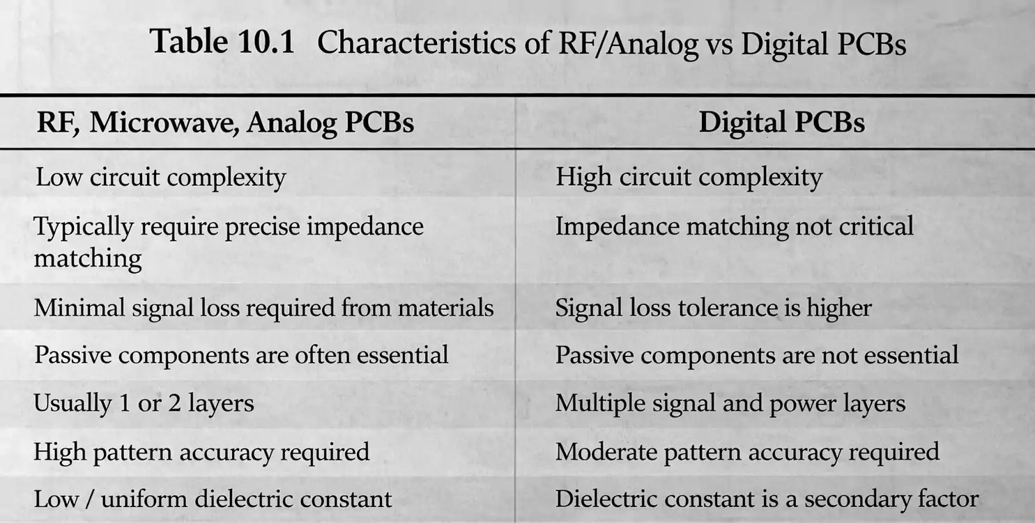
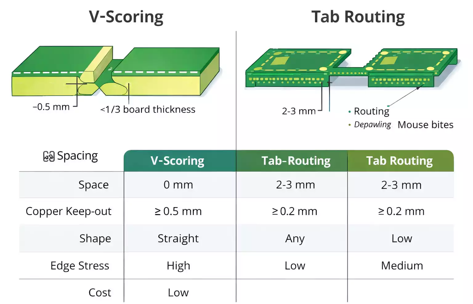
V-Cut vs Tab-Route (With Mouse Bites) — Choosing by Rules, Not Guesswork
V-Scoring (V-Cut)
A V-cut uses angled blades to create a thin groove along the entire panel line.
Boards remain connected by a small wedge of fiberglass, usually about one-third of the board thickness.
It’s the fastest and cheapest option for straight-edge, rectangular designs.
However, V-cuts cannot follow curves and generate higher mechanical stress during separation.
Sensitive components should stay at least 3 – 4 mm away from the scoring line.
Tab-Routing and Mouse Bites
Tab routing uses a small milled channel around each board, leaving thin bridges to hold pieces together.
Each bridge often has 3–5 drill holes (mouse bites) that weaken it and lead to later breakage.
Advantages:
- Works with curved or irregular shapes.
- Allows components closer to the edge (less stress).
- Cleaner outer profile after sanding.
Quick Decision Tree
| Straight edges, rectangular layout | V-cut |
| Irregular shape or edge components | Tab-route |
| Need perfect appearance | Routing or laser |
| Very thin boards | Tab-route or laser |
| High-volume production | V-cut (faster) |
For a visual comparison of scoring and routing basics, see the earlier FastTurn article on V-Score vs Tabs.
Designing Better Mouse Bites
Mouse bites seem simple, but have a large effect on depaneling quality.
Too few holes, and the bridge resists breaking; too many, and it crumbles during reflow.
Typical parameters
- 3 – 5 holes per bridge.
- Hole diameter: 0.5 – 1.0 mm.
- Center-to-center spacing: around 0.8 – 1.0 mm.
- Bridge spacing along the board edge: every 1.5 – 3 inches, depending on board stiffness.
- Copper/component clearance: ≥ 1/8 in (3.2 mm); for fragile MLCCs, use ≥ 1/4 in (6.4 mm).
After depaneling, remove burrs with a rubber sanding wheel or fine file.
If the assembly is cosmetic (consumer front panels, LED frames), finish edges with light polishing.
SMT Throughput and Fixtures: Make the Panel Work for You
A good panel layout can improve pick-and-place speed by 10 – 20%.
Here are a few practices that production engineers rely on:
Same Orientation
Place all boards in the panel so they face the same direction.
Avoid 180° rotations — they force the machine to re-program feeder angles and AOI templates.
Vacuum Trays and Palettes
Thin, narrow, or irregular boards can sag or twist under the pressure of a conveyor.
A custom vacuum or aluminum fixture keeps them flat during reflow and wave soldering.
When V-cuts weaken panel rigidity, add a jump scoring pattern (short uncut segments) or reinforcement rails at both ends.
Wave Solder Direction
For mixed-technology boards, align the panel's long dimension with the wave-solder flow to prevent tombstoning and solder bridges.
Leave small gaps or “thieves” at the trailing edge to absorb extra solder.
All of these actions turn PCB Panelization from a mechanical necessity into a tool for process optimization.
Depanelization and Stress Control
Once assembly is finished, every panel must be separated.
How you do it affects yield and reliability.
Common Depaneling Methods
| Hand break | Operators snap along V-groove; fastest but inconsistent. | Simple rectangular boards, prototypes. |
| Pizza cutter / rolling blade | Circular blade runs through scoring lines. | Volume production of scored panels. |
| Routing / milling | Spindle follows contour, minimal mechanical shock. | Irregular or sensitive boards. |
| Laser cutting | High precision, no physical stress, higher cost. | Thin, complex, or appearance-critical PCBs. |
Reducing Stress and Damage
- Keep components and traces away from cut lines (see distances in the DFM table below).
- Use support pallets or fixtures when breaking panels.
- Depanel in one continuous motion rather than twisting back and forth.
- For multi-layer or thin substrates, pre-heat slightly to reduce fiber cracking.
- Inspect edges under magnification for fiber pulls or pad lifting.
Quick DFM Checklist and Recommended Dimensions
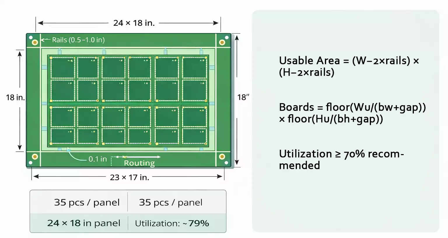
| Panel size (overall) | Around 18 × 24 in industry standard | Matches printers and conveyors |
| Edge rails width | 0.2 – 0.4 in (5 – 10 mm) | Space for fiducials, labels, tooling holes |
| Fiducial diameter | 1 – 3 mm, with 1 mm mask clearance | Three asymmetrical marks preferred |
| Tooling hole | Ø 3 mm | Keep ≥ 2 mm away from copper |
| Board-to-board spacing | 0 mm (V-cut) / ≈ 2 mm (routing) | Adjust per cutting method |
| Copper to cut line | ≥ 0.5 mm (V-cut) / ≥ 0.2 mm (routing) | Prevent exposed copper |
| Component to cut line | ≥ 1–2 mm (general) / ≥ 3–4 mm for V-cut | Avoid cracking solder joints |
| Mouse bites | 3–5 holes, Ø 0.5–1 mm, 0.8–1 mm pitch | Leave smooth edge after sanding |
| Rails fiducials/holes | 2–3 fiducials + 2 tooling holes | For accurate pick-and-place alignment |
Always verify these numbers with your fabrication and assembly house, as machine tolerances differ.
Common Production Issues and How to Fix Them
1. Edge Chipping or Fiberglass Burrs
→ Check residual material on scoring lines; widen the uncut web slightly or fine-tune milling feed.
Use gentle sanding after a break.
2. Cracked Solder Joints
→ Increase the distance between components and the nearest cut line; use depaneling fixtures to distribute stress evenly.
3. Board Warp or Twist
→ Add jump-scoring sections or reinforcement rails; balance copper density across layers; control cooling rate after reflow.
4. AOI Mis-alignment
→ Ensure fiducials are clean, open, and far enough from routing dust; never cover them with solder mask or silkscreen.
Frequently Asked Questions
Q1: How small should a PCB be before it requires panelization?
A: Anything smaller than about 50 × 50 mm should be grouped into a panel.
Irregular or narrow boards also benefit from panel rails for conveyor stability.
Q2: Are there “golden” panel sizes?
A: Most assemblers prefer panels close to 18 × 24 inches, with ½ to 1 inch margins.
These fit common printers, conveyors, and reflow ovens.
Q3: What are the hard limits for V-cuts?
A: Lines must be straight and continuous; spacing ≥ 2 mm; typical board thickness ≥ 0.6 mm; avoid more than 25 lines per direction.
Final Thoughts
PCB Panelization is both an art and an engineering science.
A small decision — where to place a fiducial, how wide to make a rail, or how many holes to drill in a tab — can decide whether production runs smoothly or turns into a bottleneck.
And when you need expert support for small-batch or quick-turn projects, FastTurn PCB offers complete design-for-assembly review and PCB Panelization optimization to keep your build on schedule.