PCB LED design influences brightness uniformity, thermal stability, electrical efficiency, and overall lifespan. An LED PCB is a specialized circuit board for powering LEDs and managing heat, both of which are vital for maintaining performance and longevity.
A well-designed LED PCB board must manage three core factors simultaneously:
- Uniform current distribution
- Efficient heat dissipation
- Stable, low-impedance routing
When any one of these is neglected, lighting performance and reliability suffer. In higher-density designs, the challenge becomes even greater because compact layouts increase thermal density, making it even harder to maintain current flow. High-density LED PCB design, therefore, depends on careful space optimization, current balancing, and heat control rather than simply fitting more LEDs onto the board.
What Is an LED PCB Board?
An LED PCB board is a printed circuit board specifically designed to support LEDs both electrically and thermally. Unlike standard PCBs used mainly for signal processing or lower-power electronics, LED boards must handle sustained current and significant heat generation. In many lighting products, the PCB itself becomes part of the thermal management system.
Depending on power level and application, common substrate options include:
- FR-4 – suitable for low-power or indicator LEDs
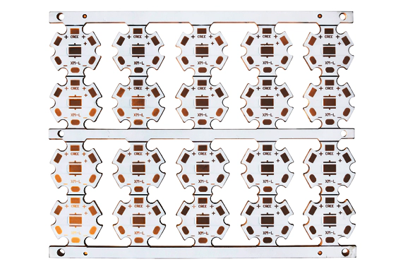
- Aluminum-core PCB (MCPCB) – widely used for general lighting
- Copper-core PCB – used for higher thermal loads
- Ceramic PCB – used for high-reliability or high-temperature environments
Metal-core and ceramic substrates are preferred for PCB LED guides to provide strong heat dissipation and structural reliability in high-power applications.
An additional point worth emphasizing is that LED PCBs are often built as layered thermal structures rather than just flat electrical carriers. In metal-core boards, the stack-up typically includes a copper circuit layer, a thermally conductive dielectric, and a metal base, allowing heat to move away from the LED much faster than in ordinary FR-4 designs.
PCB LED Core Design Objectives
A reliable LED PCB board must achieve three major design goals.
1. Uniform Brightness
Current must be evenly distributed across all LEDs or branches. If the routing impedance is unbalanced, some LEDs may receive more current than others, resulting in visible brightness variation and uneven aging. High-density LED designs consistently stress that even current flow is a major factor in maintaining uniform output.
2. Effective Thermal Control
Efficient heat transfer from the LED junction to the air is critical. Excessive temperature causes lumen degradation, color shift, packaging stress, and reliability problems. Metal substrates are used in high-power lighting to reduce LED temperature and improve reliability under thermal stress.
3. Controlled Voltage Drop
Trace resistance must be minimized to avoid visible dimming, especially in long LED strips or boards with higher current. This becomes especially important in linear lighting, signage, and high-density modules, where small voltage differences along the power path can translate directly into uneven brightness.
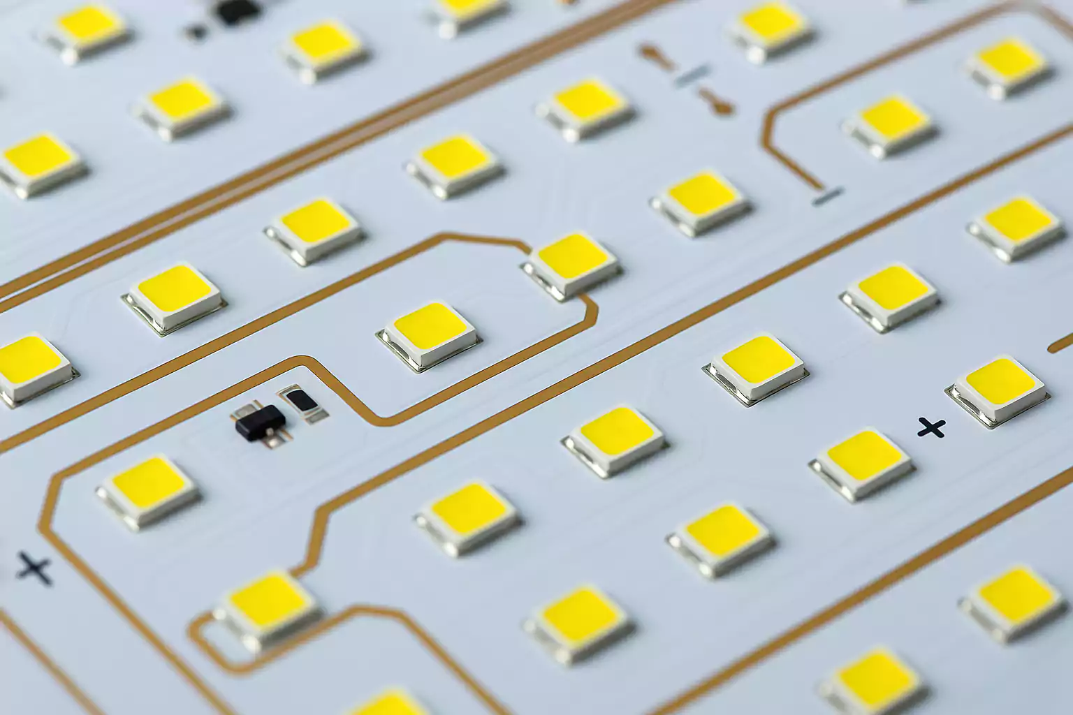
LED Symmetry and Spacing
LED placement directly influences both optical and thermal performance.
1. Symmetry
LED arrays should be arranged symmetrically around the mechanical or optical center of the board. Symmetry helps equalize:
- Electrical path length
- Thermal path length
- Light distribution
Balanced geometry reduces variation between center and edge LEDs, improving overall uniformity.
2. Spacing
LED spacing must support:
- Smooth light blending
- Adequate thermal spreading
- Manufacturable routing and pad clearances
If spacing is too large, dark zones appear; if too tight, hotspots form and routing becomes difficult. Adequate spacing between metals, pads, and traces not only improves optical performance and manufacturability but also reduces board errors.
High-density layouts require stronger thermal paths and more disciplined current distribution. A tightly packed board may increase lumen density, but without enough copper area and heat transfer capacity, the gain in compactness can come at the cost of reliability.
Driver IC Placement and Power Architecture
Driver placement significantly influences voltage drop, electrical stability, and efficiency.
1. Keep the Driver Close to the LED Load
Shorter trace length means:
- Lower resistance
- Reduced power loss
- Improved current stability
The driver-to-load path should remain short and direct whenever possible.
2. Select the Right Drive Method
LED PCB design commonly uses either constant-current (CC) or constant-voltage (CV) driving, and the correct choice depends on the LED type and the intended circuit architecture. Constant-current driving is generally preferred for maintaining stable LED current and more consistent brightness.
3. Define a Clear Power Structure
Use a main trunk with symmetric branches:
- Main trunk → low-impedance backbone
- Branches → equal geometry and resistance
In long LED boards, consider dual-end power injection to minimize end-of-line dimming.
For higher-density boards, a well-planned power architecture also helps prevent localized overload, especially when multiple strings or clustered LED groups share the same source path.
Thermal Pad Positioning and Heat Path Design
Thermal design must be continuous and intentional. A typical heat-flow path is:
LED junction → thermal pad → copper layer → thermal vias → backside copper or heatsink → ambient air
If any part of this chain is interrupted, temperature rises locally.
Key considerations include:
- Align thermal pads with the primary heat-spreading copper.
- Avoid isolating pads near board edges.
- Prevent mounting holes or slots from breaking copper continuity.
Thermal design must be planned during layout, not added afterward.
Another practical consideration is board dimensioning. LED PCB design references note that board size, component placement, and base material should be chosen with heat transfer in mind, as thermal performance is strongly tied to the available area for copper spreading and heatsink contact.

Copper Pour Continuity and Thermal Via Arrays
Copper serves two purposes in an LED PCB:
- Electrical conduction
- Thermal spreading
1. Copper Continuity
Avoid:
- Narrow neck-down areas
- Unnecessary splits
- Isolated copper islands
These features create thermal bottlenecks and concentrate current.
2. Thermal Via Arrays
Thermal vias transfer heat vertically through the board. Best practices include:
- Evenly distributed via arrays under thermal pads.
- Full coverage of heat-generating areas
- Direct thermal connection to the backside copper or heatsink
If thermal vias and copper pours cannot sufficiently reduce temperature, a metal-core or ceramic substrate may be required.
In high-power LED structures, the dielectric layer between copper and the metal base is also a critical factor. Metal-core LED boards typically rely on thermally conductive dielectric materials, and available guides describe these layers as spanning a range of thermal conductivities, which means material choice within the stack-up can influence performance almost as much as via count or copper area.
Routing Principles for LED PCBs
Routing quality directly affects electrical stability, EMI performance, and consistent visible lighting.
1. Minimize Current Loop Area
A large current loop increases parasitic inductance and noise. Keep supply and return paths:
- Short
- Direct
- Closely paired
2. Paired Supply and Return Routing
Route V+ and GND close together to reduce loop inductance and improve electromagnetic stability.
3. Avoid Current Detours
Unnecessary bends and long paths increase:
- Resistance
- Voltage drop
- Heat generation
Efficient routing improves both brightness consistency and electrical reliability.
For practical LED products such as flashlights and compact lighting modules, design guidance consistently points to short current paths and wider power traces as direct ways to reduce voltage loss and improve efficiency.
Series vs. Parallel LED Routing
Different connection types require different routing strategies.
1. Series LEDs
- The same current flows through each LED
- Focus on the predictable voltage drop.
- Use equal-width traces
Series routing is generally simpler, but the total forward voltage must be carefully managed.
2. Parallel LEDs
- Higher risk of current imbalance
- Requires symmetric routing
- Match trace length, width, and via count.
3. Mixed Series-Parallel Designs
- Use a low-impedance main bus.
- Connect each branch symmetrically.
- Balance branch impedance carefully
Parallel imbalance remains one of the most common causes of uneven brightness and thermal mismatch in LED boards.
This is especially true in high-density LED layouts, where branch-to-branch differences can become amplified because thermal and electrical conditions vary more rapidly across a compact area.
Trace Width, Copper Weight, and Voltage Drop
Trace design must match current requirements.
1. Trace Width
High-current paths require wider traces than signal lines. Narrow traces increase resistance and self-heating.
2. Copper Weight
Heavier copper improves:
- Current capacity
- Thermal spreading
- Voltage stability
Long LED strips are particularly sensitive to voltage drop. If power enters only from one end, brightness may decrease at the far end.
Solutions include:
- Wider trunk traces
- Thicker copper
- Dual-side power injection
Another useful takeaway from recent PCB LED references is that trace width should not be considered alone. Copper thickness, board length, current magnitude, and thermal environment all interact, so the optimal design choice is usually a combination of wider traces, better copper spreading, and a more suitable substrate rather than a single adjustment.
COB LED PCB vs. Standard LED PCB
COB (Chip-on-Board) LED PCBs integrate multiple LED chips onto a single substrate.
Advantages include:
- Higher light density
- Improved optical uniformity
- More compact structure
Challenges include:
- Higher thermal density
- More demanding heat management
- Greater dependence on substrate performance
COB boards typically require stronger substrate materials and more aggressive thermal design than standard SMD LED boards. Because light-emitting chips are more tightly packed, COB structures often benefit disproportionately from high-performance base materials, efficient dielectric layers, and very short heat paths.
Additional Design Factors Often Overlooked
To make an LED PCB truly robust, several secondary design factors should also be reviewed early:
- Board dimensions and mechanical envelope, because these affect copper area and heatsink attachment options
- Component tolerances and clearances, which influence assembly quality and reduce layout errors
- Application environment, such as automotive, outdoor, or enclosed fixtures, because ambient temperature changes the required thermal margin
- Structural reliability under thermal cycling, since high-power LED boards experience repeated heating and cooling during operation
These may not always appear in short PCB LED overviews, but they become critical in real product development.
Common LED PCB Design Mistakes
Most LED PCB reliability issues stem from a small set of repeated design mistakes:
- Uneven LED spacing
- Poor driver placement
- Broken thermal paths
- Narrow high-current traces
- Asymmetrical parallel routing
- Inadequate substrate selection
Final Thoughts
LED PCB design results from disciplined coordination among placement, routing, thermal management, and material selection. When current paths are optimized, heat flow is continuous, and the substrate matches the power demand, the board delivers stable brightness, controlled temperatures, and predictable long-term performance. Across current LED PCB design guidance, high-performance lighting depends on treating the PCB as both an electrical platform and a thermal structure.
For teams building high-performance LED products, that systems-level approach is what turns a board from a simple carrier into a reliable lighting platform. FastTurnPCB provides precision manufacturing support for high-performance LED PCB applications.