


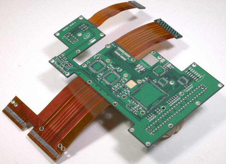
When you look at a printed circuit board (PCB), you mostly see a flat green plate with shiny copper pads and thin tracks. But underneath that surface lies a carefully built sandwich of copper and insulating materials—called PCB layers.
These layers control how signals move, how power is distributed, and how stable your board will be.
This guide explains what PCB layers are, how they’re stacked, how many you really need, and how to tell how many layers a board has.

Quick Overview: What Are PCB Layers and Common Layer Counts
A PCB layer is one conductive copper sheet or supporting layer in the board’s structure. Layers are laminated together with insulating dielectric materials to create a complete circuit board.
Most PCBs have an even number of layers—usually 2, 4, 6, or 8—to keep the stack symmetrical and easy to manufacture.
| 2-layer | Simple controllers, LED drivers, low-speed IoT boards | Low cost, fast turnaround | Limited routing space, poor EMI control |
| 4-layer | Consumer electronics, USB or HDMI interfaces | Better signal integrity, solid ground plane | Slightly higher cost |
| 6-layer | Industrial, automotive, mid-speed data buses | Good EMI control, dense routing | More expensive and harder to rework |
| 8-layer | High-speed computer boards, motherboards | Excellent impedance and shielding | High manufacturing cost |
What “Layers” Actually Mean in a PCB
Each PCB consists of conductive and non-conductive layers.
Here’s what each one does:
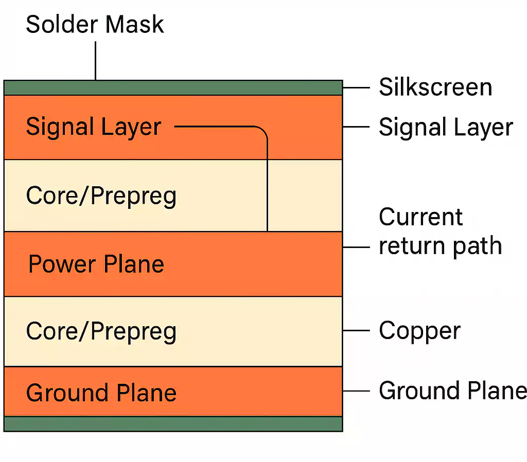
- Signal layers – Carry electrical signals between components. They include traces and vias that link different nets.
- Ground planes (GND) – Provide a low-impedance return path for signals and help shield against electromagnetic noise.
- Power planes (PWR) – Distribute voltage to ICs evenly and lower the voltage drop across the board.
- Core and prepreg – These are fibreglass-reinforced dielectric materials (often FR-4) that separate copper layers and define the board’s thickness.
- Solder mask – The green (or blue, red, black) coating that insulates and protects copper from oxidation and solder bridges.
- Silkscreen – The white text or symbols used to mark components, reference designators, or logos.
A cross-section diagram of a PCB would show copper layers alternating with insulating layers, much like a layered cake. The copper forms the electrical circuits, while the dielectric provides mechanical strength and insulation.
Common PCB Stack-ups and How They Work
The stack-up defines the order and spacing of all copper and dielectric layers.
Good stack-up design reduces noise, improves impedance control, and minimises electromagnetic interference (EMI).
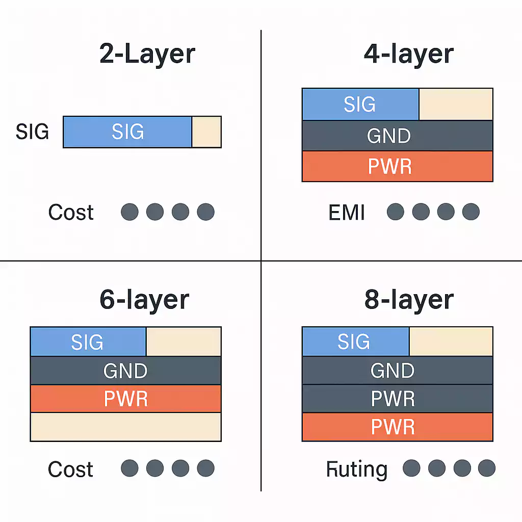
2-layer PCB
The simplest structure: Top layer + Bottom layer.
Both sides can carry components and copper traces. Designers use wide traces and ground pours to help with current return paths.
Pros: Cheapest, fastest to fabricate.
Cons: Limited routing space; difficult to control EMI or impedance.
4-layer PCB
The most popular choice for modern electronics.
Typical configuration:
- Layer 1: Signal (Top)
- Layer 2: Ground Plane (GND)
- Layer 3: Power Plane (PWR)
- Layer 4: Signal (Bottom)
This layout provides solid reference planes between signal layers, helping with signal integrity and EMI control. It’s ideal for high-speed USB, HDMI, or microcontroller boards.
6-layer PCB
Used when more routing density or isolation is required.
Common setup: SIG – GND – SIG – PWR – GND – SIG.
Two ground planes provide shielding, while the inner signal layer can handle differential pairs or sensitive analogue routing.
This stack-up is widely used in automotive and industrial control systems.
8-layer PCB
High-speed computing and motherboard designs often use 8 layers.
A possible configuration:
SIG – GND – SIG – PWR – GND – SIG – GND – SIG.
Multiple reference planes reduce crosstalk and improve impedance control across differential pairs like PCIe, DDR, or USB 3.0.
How to Decide How Many Layers You Need
Choosing the right layer count depends on several design factors. Here’s a quick decision map engineers often use:
- Signal speed and type –
- < 100 MHz, simple analogue or low-speed logic → 2-layer.
- 100 MHz–1 GHz digital interfaces (USB 2.0, Ethernet) → 4-layer.
- > 1 GHz high-speed differential pairs (USB 3.x, PCIe, HDMI) → 6 or 8 layers.
- Component density and board size –
More components and smaller boards need more routing layers. - Power and ground distribution –
Dedicated planes reduce voltage noise and improve stability. - Electromagnetic interference (EMI) –
Shielded reference planes and tight coupling between signal and return paths improve EMC performance. - Budget and lead time –
Fewer layers mean lower cost and faster manufacturing.
Why Multilayer PCBs Are Usually Even-Layered
If you look at manufacturing catalogues, you’ll notice that most PCBs have an even number of layers—and there’s a good reason for that.
Manufacturing efficiency
Odd-layer boards require one copper foil to be left unpaired during lamination. This means additional process steps and uneven mechanical stress, which increase costs and risks.
Mechanical balance
Symmetrical layer stacks prevent board warping during heat cycles.
If one side has more copper or resin, the PCB bends slightly after soldering. Even layers keep both sides equal and stable.
Electrical performance
Pairs of signal and reference planes make impedance more predictable and reduce return paths, improving overall signal quality.
That’s why you rarely see 3- or 5-layer PCBs in production—fabricators almost always recommend converting them to 4 or 6 layers instead.
How to Identify the Number of Layers in a PCB
Knowing how many layers a board has is useful when repairing, reverse-engineering, or creating documentation.
Here are several ways to figure it out.
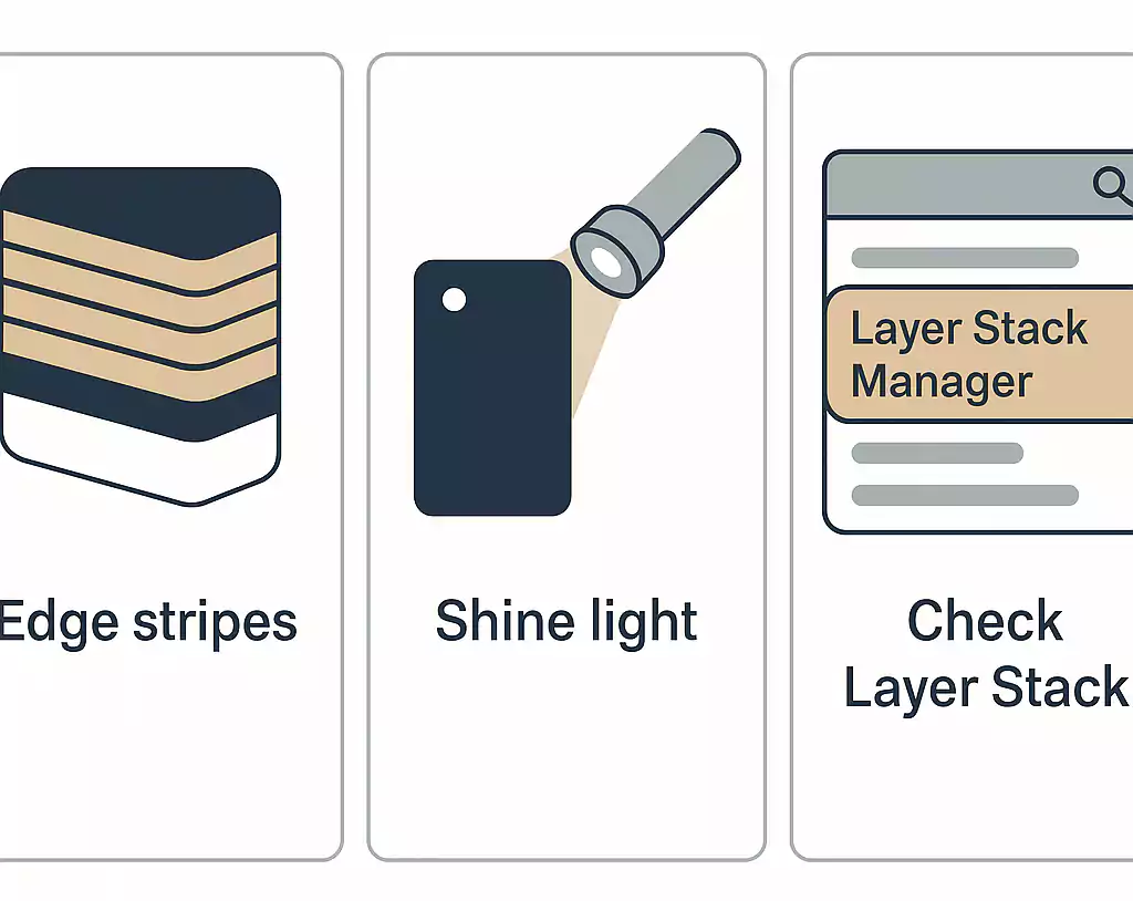
1. Visual inspection (no tools needed)
- Look at the board edge: You may see thin “stripes” that represent copper and dielectric layers.
- Shine a light through the board: Two-layer PCBs allow light to pass through traces more easily, while multilayer boards look darker and more opaque.
- Check for via depth: Blind or buried vias (not passing through the entire board) often indicate multiple inner layers.
2. Using design files
If you have the Gerber or ODB++ files, each copper layer will have its own file (e.g., Top.GTL, Inner1.GBL, Bottom.GBL, etc.).
Count the copper files to know the exact layer number.
3. Using CAD software
In Altium Designer, go to Design → Layer Stack Manager to see all defined layers and dielectric thicknesses.
In KiCad, open Board Setup → Layers, and you’ll find the stack structure.
In Autodesk Fusion 360, the Layer View shows the same information as the PCB workspace.
4. Advanced or destructive methods
For detailed analysis, manufacturers sometimes cut a cross-section of the PCB and observe it under a microscope or CT scanner.
This is used in quality control or failure analysis rather than routine inspection.
How Many Layers Do Motherboards Have?
PC motherboards and server boards are complex, high-speed systems that need many dedicated planes for power, ground, and signal routing.
- Consumer motherboards usually have 6–12 layers.
- Workstation and server boards can reach 14–16 layers or more.
These extra layers are used for multiple power domains (CPU, GPU, memory), impedance-controlled differential pairs, and shielding between sensitive nets.
However, more layers do not always mean “better.” A well-optimised 6-layer board can outperform a poorly designed 8-layer one if the stack-up and routing are carefully planned.
FAQ
1. How many layers can a PCB have?
Standard PCBs use 1 to 16 layers, but advanced boards can exceed 30 or even 100 layers in aerospace or telecom systems.
2. What’s a typical 4-layer stack-up?
A common setup is Signal – Ground – Power – Signal, providing stable reference planes for controlled impedance routing.
3. Why are multilayer PCBs usually even-layered?
Even layers keep the board mechanically balanced, easier to manufacture, and electrically consistent.
4. How can I identify PCB layers without design files?
Look at the board edge for visible layer stripes, shine light through it, or check Layer Stack Manager in Altium or KiCad.
Conclusion
PCB layers are the foundation of every modern electronic design.
They define how signals flow, how power is delivered, and how stable your board will be in real-world conditions.
A thoughtful layer stack-up doesn’t just make fabrication easier—it ensures your design performs reliably from the first prototype to mass production.
