

On every printed circuit board (PCB), the copper-clad laminate (CCL) serves as the foundation. Whether it’s single-sided or double-sided, this base material defines the board’s mechanical strength, dimensional stability, and overall electrical reliability. In short, PCB performance starts with the laminate.
Today, PCB laminates face two powerful trends that are reshaping material design and qualification testing:
- The higher-temperature demands of lead-free soldering under modern RoHS compliance regulations.
- The need for superior signal integrity in high-speed, high-frequency applications, such as 10-Gigabit Ethernet.
This article explores how both factors influence laminate performance and explains what to focus on when selecting and testing PCB base materials in modern manufacturing environments.
RoHS Compliance and Lead-Free Soldering: Surviving the Heat
The RoHS (Restriction of Hazardous Substances) directive, implemented by the European Union, prohibits the use of certain toxic substances, including lead, in electronic products. As a result, the electronics industry has shifted primarily from traditional tin-lead soldering to lead-free soldering.
While this transition is environmentally beneficial, it also significantly increases thermal stress on PCB laminates.
1. Higher Soldering Temperatures Push Material Limits
Traditional tin-lead solder has a melting point near 183 °C, with typical reflow peaks around 220 °C. In contrast, lead-free soldering can reach 260 °C, roughly 30–40 °C higher than lead soldering.
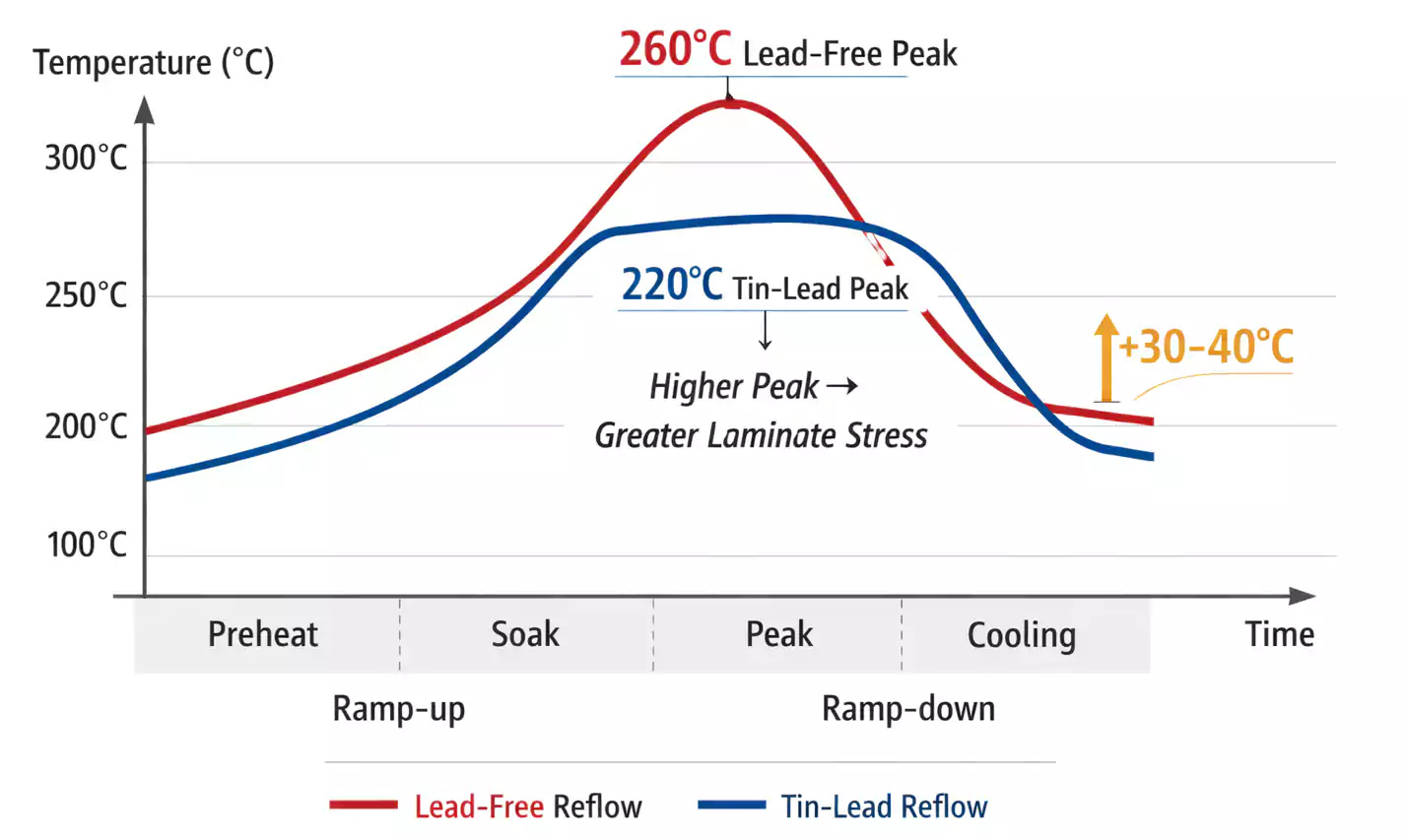
Most PCBs must now withstand five or more reflow cycles, and complex assemblies may experience six or more. Each additional cycle compounds thermal fatigue.
A well-known rule of thumb states that every 10 °C rise in temperature doubles the rate of resin degradation. This increased stress heightens the risk of delamination or “popcorning” during reflow.
To survive these conditions, modern laminates must feature:
- Higher decomposition temperature (Td)
- Improved thermal stability
- Enhanced mechanical integrity under cyclic heating
These changes have also prompted engineers to re-evaluate existing laminate test methods to ensure they reflect real lead-free process conditions.
2. PCB Reliability Under Lead-Free Stress
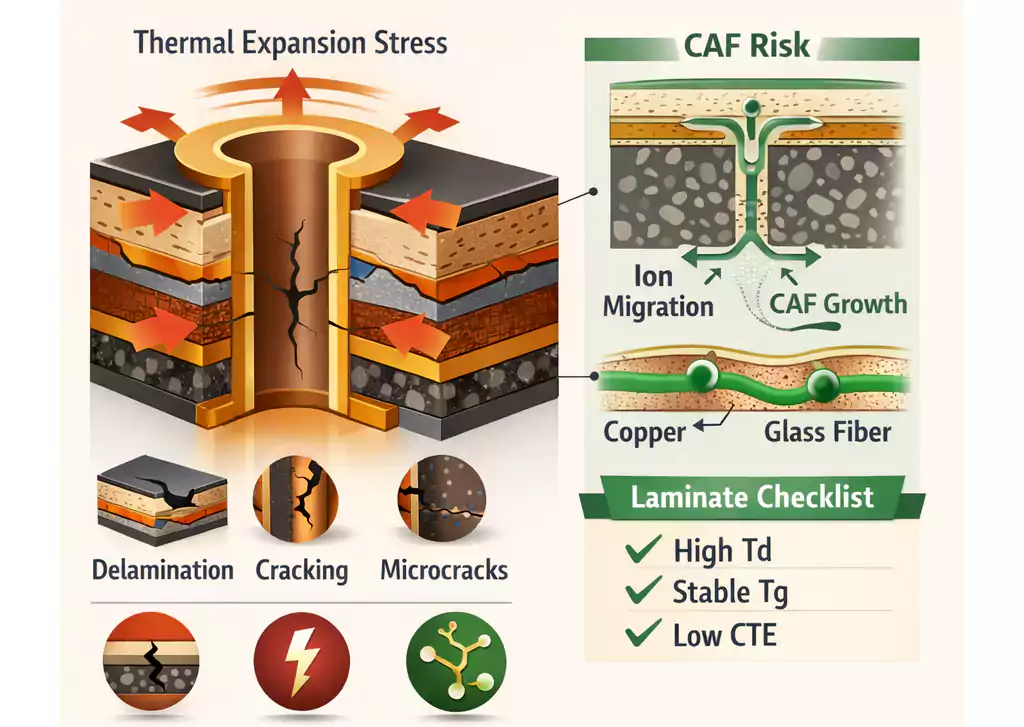
Even when the same laminate material and reflow count are used, the higher peak temperatures of lead-free soldering significantly increase the thermal expansion stress in plated-through holes (PTHs).
This elevated stress can lead to micro-cracking, interlayer separation, or open vias over time. To maintain reliability comparable to traditional soldering, laminate performance must evolve.
Key reliability-critical properties include:
- Interlayer adhesion strength
- Resistance to conductive anodic filament (CAF) growth
- Dielectric strength
- Thermomechanical stability — including peel strength, glass transition temperature (Tg), and coefficient of thermal expansion (CTE).
None of these properties should degrade during 260 °C lead-free reflow.
In short: better materials are no longer optional—they’re essential for reliability.
10-Gigabit Ethernet and the Rise of High-Speed, High-Frequency Design
As Ethernet moves from gigabit to 10-gigabit data rates, high-speed signaling has become standard. Signal integrity (SI) is now a primary design consideration, and PCB laminate materials play a central role in it.
1. Electrical Demands: Low Dk and Low Df
High-speed transmission depends heavily on the laminate’s dielectric constant (Dk) and dissipation factor (Df) (sometimes referred to as dielectric loss, Dr).
- Lower Dk → faster signal propagation and easier impedance control.
- Lower Df → reduced transmission loss and cleaner eye diagrams.
In a 10 Gbps channel, even a small change in loss tangent (e.g., Df = 0.005 → 0.003) can make or break the link margin.
For this reason, modern PCB laminates often use advanced resin systems—modified epoxies, polyimides, PTFE blends, or hybrid materials—to achieve the necessary balance of low Dk/Df and processability.
2. Design and Manufacturing Challenges
Beyond material selection, high-speed design requires tight control of PCB structure and fabrication precision.
Critical factors include:
- Impedance control: consistent line width, dielectric thickness, and copper roughness.
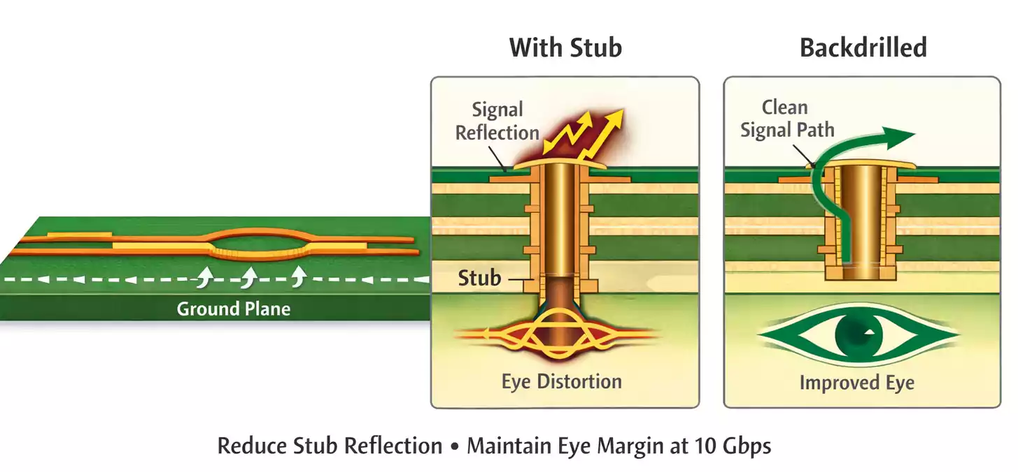
- Via stub minimization: reducing signal reflection and distortion.
- Layer-to-layer registration: ensuring consistent geometry for differential pairs.
Together, these requirements demand laminates with stable dielectric properties, uniform thickness, and excellent process reliability.
From Datasheet to Real-World Validation
Laminate manufacturers typically provide comprehensive datasheets listing Dk, Df, Tg, Td, CTE, and other key values. These serve as a good starting point for material evaluation, but real-world testing is still essential.
Why? Because:
- Datasheet values are often measured under ideal lab conditions.
- Actual PCB fabrication involves drilling, plating, lamination, and multiple thermal cycles.
- The mechanical and electrical stresses in production can differ significantly from those in test coupons.
To ensure real-world reliability, engineers should supplement supplier data with in-house testing on actual PCB builds.
Standard validation tests include:
- Thermal shock and delamination testing
- Dielectric property verification at relevant frequencies
- PTH reliability and CAF resistance
- Peel strength and Tg confirmation
These tests not only confirm performance but also help engineers understand how material behavior interacts with process conditions—the foundation of consistent, reliable manufacturing.
Key Takeaways: The New Mindset for PCB Laminate Evaluation
Whether it’s the high-temperature demands of lead-free soldering or the high-frequency challenges of 10-Gigabit Ethernet, the PCB laminate now plays a pivotal role in board reliability and performance.
A modern evaluation framework should address three essential dimensions:
- Manufacturing compatibility: Can the laminate endure multiple 260 °C reflow cycles?
- Signal integrity: Are Dk and Df stable and consistent across frequencies?
- Long-term reliability: Does the material resist delamination, CAF, and thermal fatigue?
In today’s environment, PCB engineers must go beyond reading datasheets—they need to interpret test results and understand the underlying physics.
After all, every copper-clad laminate (CCL) is more than just a base material; it’s the bridge connecting design intent and manufacturing reality.
FAQ
What is a PCB laminate?
A PCB laminate, or copper-clad laminate (CCL), is the base material that provides mechanical support and electrical insulation for circuit boards.
How does lead-free soldering impact laminates?
Lead-free soldering requires higher reflow temperatures (up to 260 °C), demanding laminates with better thermal stability and resistance to delamination.
What is RoHS compliance?
RoHS compliance ensures PCB materials are lead-free and capable of withstanding higher soldering temperatures without performance loss.
What laminate properties are most critical?
High Tg, Td, low CTE, and strong adhesion for reliable performance under thermal stress.
Why are special laminates needed for high-speed PCBs?
High-speed designs require low Dk and low Df laminates to ensure signal integrity and minimize loss.
What’s the key takeaway?
Choose copper-clad laminates that combine thermal endurance for lead-free soldering with stable electrical properties for high-speed applications.
