When designing a printed circuit board, the ground plane is one of the most important layers.
Although it appears simple, how you design and connect the ground plane determines whether your board performs well or suffers from noise, signal loss, or EMI.
In this guide, we’ll explain what a PCB ground plane does, why it matters for current return, EMI, and signal integrity, and how to design it for digital and RF boards.
What Is a PCB Ground Plane and Why Does It Matter?
A PCB Ground Plane is a large copper area used as a common electrical reference for all signals and power.
It provides a low-impedance path for return currents, reduces electromagnetic noise, and spreads heat across the board.
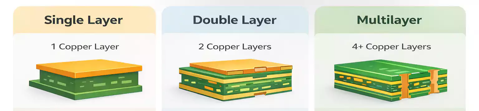
In multilayer PCBs, the ground plane is often a dedicated copper layer right below or above the main signal layer.
In two-layer boards, it may be a poured copper area on the bottom side that connects to GND.
A solid ground plane improves:
- Signal integrity
- Power stability
- EMI/EMC performance
- Mechanical strength and thermal spreading
Without it, return currents take longer paths, increasing loop area and radiation.
Return Path: The First Rule of a Good Ground Plane
Every signal that goes out must come back through a return path—usually the PCB Ground Plane.
For high-frequency signals, return current follows the path of least impedance directly under the trace, rather than the shortest physical route.
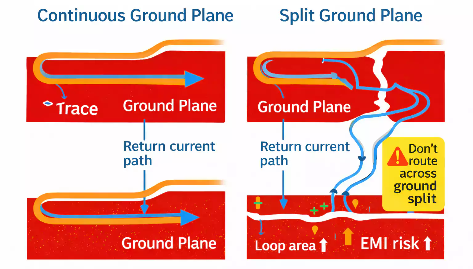
When the ground plane is continuous, the return path is smooth and predictable.
But if there’s a gap, split, or missing copper under a trace, the return current must detour around it, creating a large loop area.
This leads to:
- Higher loop inductance
- Crosstalk and reflections
- Increased EMI radiation
Always keep the reference plane continuous and add stitching vias when the signal changes layers so that the return current can flow nearby.
Don’t Split the Ground Plane
Splitting ground planes—such as separating analog and digital grounds—is a common layout mistake.
Why it’s risky:
- Return currents get blocked by the split and flow around it.
- This results in higher impedance and noise coupling.
- High-speed signals crossing a split cause strong EMI and timing errors.
When it’s acceptable:
- Safety isolation (high-voltage vs. low-voltage circuits)
- Sensitive analog areas (low-frequency, low-current signals)
- RF and power isolation zones where grounding must be separated by design
If you do split, connect the grounds at a single controlled point (a “star ground” or “net tie”)—not with a random trace or capacitor bridge.
Never route high-speed or clock lines over a split gap.
Layer Stack-Up: Using Ground Planes the Right Way
A smart stack-up design is the foundation of signal integrity.
Typical 4-layer configuration:
- Top: Signals
- Layer 2: Ground Plane
- Layer 3: Power Plane
- Bottom: Signals
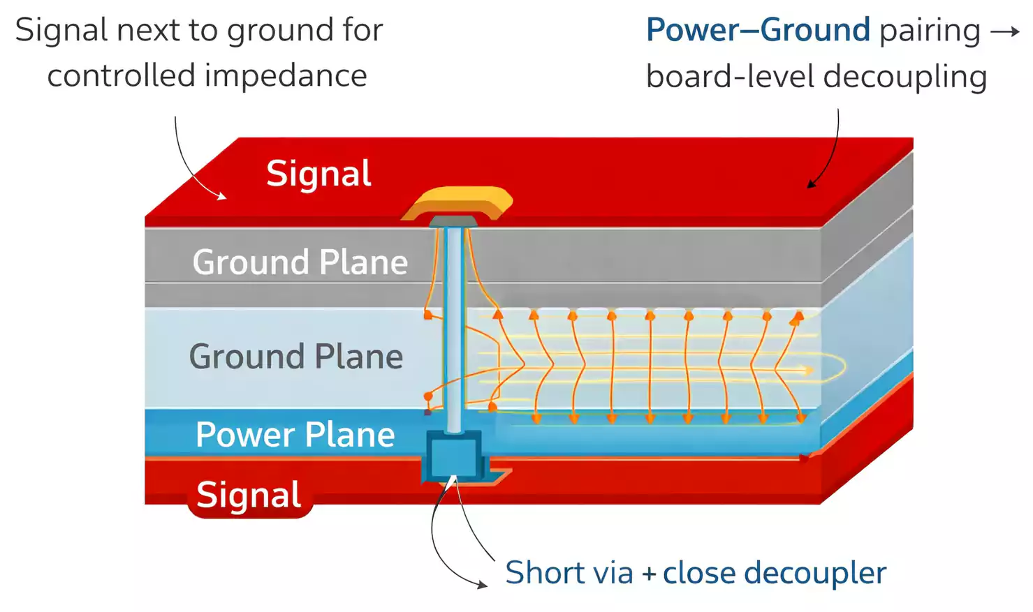
This allows every trace on the top to have a close reference plane, minimizing loop area and EMI.
In 6- or 8-layer boards, multiple ground planes boost signal return and thermal balance.
Also, placing the power and ground layers next to each other forms a natural parallel-plate capacitor, improving power delivery and decoupling performance.
In 2-layer boards, always dedicate one side mostly to ground and avoid cutting it into small islands.
EMI and EMC: The Ground Plane’s Role in Noise Control
Good grounding is the first line of defense against electromagnetic interference (EMI).
Follow these key rules:
- Keep the ground plane continuous under all high-speed traces.
- Avoid crossing split gaps with any signal.
- Minimize the current loop area between the signal and the return.
- Place decoupling capacitors close to IC power pins to connect high-frequency return currents directly to the ground.
For connectors such as USB, HDMI, or Ethernet, maintain a solid ground reference beneath the interface.
Avoid any cutouts or voids under connectors, as they increase common-mode noise.
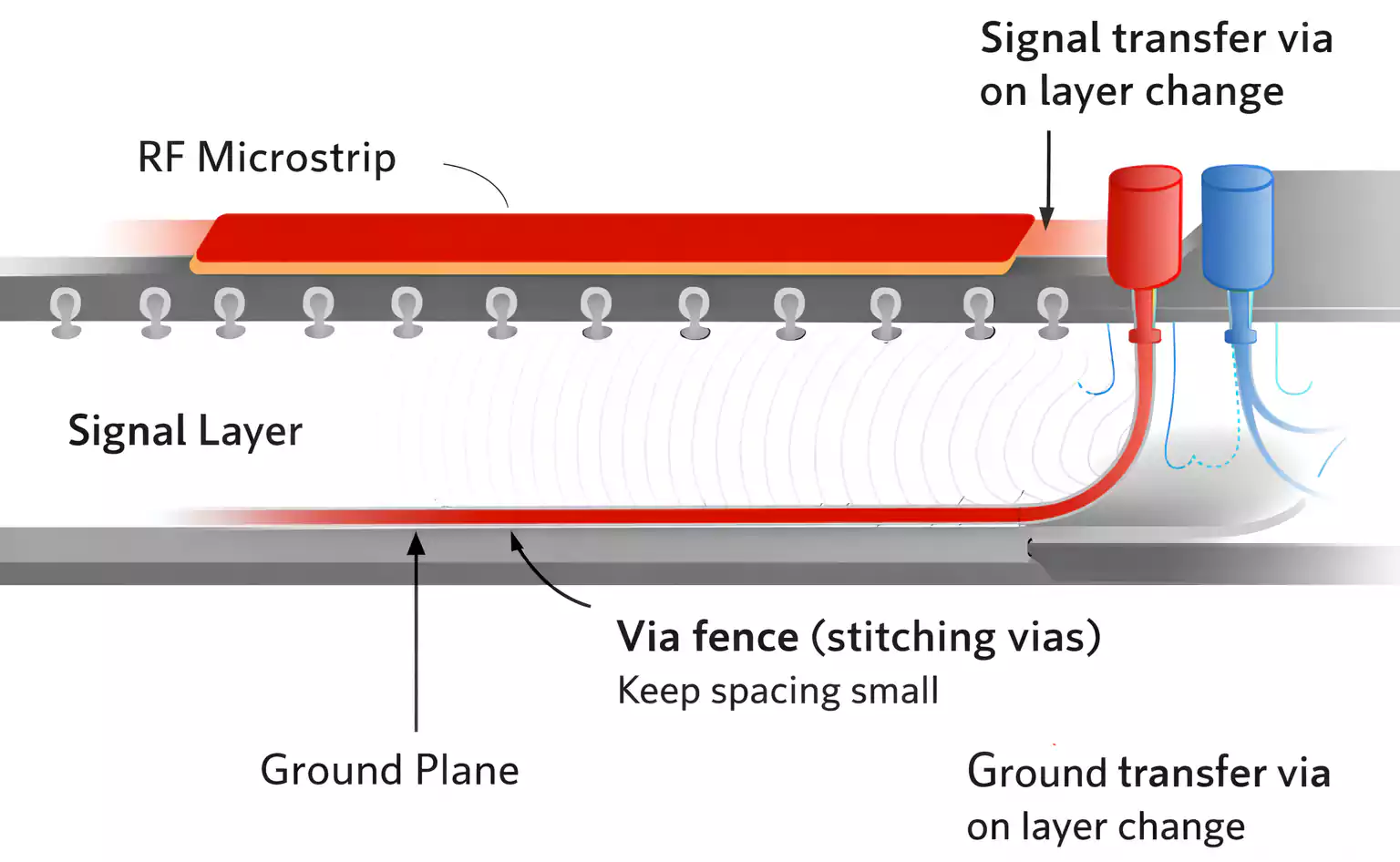
RF PCB Grounding: Microstrip, Stripline, and Via Stitching
In RF and microwave designs, the PCB Ground Plane is even more critical.
Every transmission line—microstrip (outer layer) or stripline (inner layer)—needs a continuous reference plane to control impedance and minimize radiation.
Use via stitching or via fences along the edge of RF traces or enclosures.
These create a “wall” of grounded vias that prevent energy from leaking into nearby circuits.
Choose materials carefully:
Low-loss laminates (PTFE, Rogers, or hybrid FR-4) maintain a stable dielectric constant and reduce signal loss.
Keep dielectric thickness consistent between the RF trace and ground plane to maintain impedance accuracy.
Copper Pour vs. Solid Ground Plane
When you can’t dedicate a full ground layer—like in two-layer boards—you can use copper pour to fill unused space and tie it to ground.
Tips:
- Remove or connect isolated copper islands with vias to prevent them from acting as antennas.
- Use thermal relief pads for easy soldering, but solid connections for power paths.
- Avoid “meshed” or “grid” ground fills on high-speed layers—solid copper performs better.
A solid ground layer is superior for high-speed or dense designs, offering predictable impedance and shielding.
Stitching Vias and Ground Connections
When a signal trace switches layers (for example, from top to bottom), the return path must also follow.
Add a ground via near each signal via to provide a direct return path for the current.
In high-frequency areas, place stitching vias every 5–10 mm (0.2–0.4 inch) along the edge of ground fills or near high-speed traces.
For shielding or RF zones, via fences can be spaced even closer—about one-tenth of the signal wavelength.
Avoid large gaps or cutouts in the ground near these vias, which can create impedance jumps.
Layout Rules for Mixed-Signal and Power Areas
Mixed-signal boards (analog + digital) should physically separate noisy and quiet sections, not electrically.
- Group analog, digital, and power circuits into their own zones.
- Keep high-di/dt switching loops small and close to their decoupling capacitors.
- Route sensitive analog traces only over the analog reference area.
- Use a single-point connection between analog and digital grounds.
For multilayer boards, let signal layers sit next to ground whenever possible.
Stacking power and ground planes together improves power integrity and EMI suppression.
Common Ground Plane Mistakes and How to Fix Them
| EMI test failure | Split or gaps under signal paths | Restore solid ground; add stitching vias |
| Signal distortion or ringing | Discontinuous reference plane | Use closer ground layer; check impedance |
| Crosstalk between traces | Shared return paths | Separate signals or add ground traces/vias |
| Unstable analog readings | Shared noisy digital ground | Isolate zone, connect with single point |
| Unexpected RF radiation | Floating copper island | Remove or tie island to main ground |
Conclusion
A PCB ground plane is the foundation of signal integrity, EMI control, and power stability.
Keep it continuous, close to your signals, and well-connected.
Avoid unnecessary splits, and always give your return current a short, low-impedance path home.
Whether you’re designing a digital prototype or an RF module, mastering ground planes means fewer surprises, cleaner signals, and a more reliable product.