


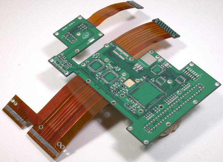
Introduction
PCB etching is the process of removing excess copper from a printed circuit board to define precise circuit patterns. It plays a critical role in both prototyping and large-scale PCB manufacturing.
This article explores two main approaches: DIY methods, often used by hobbyists for quick, low-cost results, and industrial techniques, designed for accuracy, repeatability, and high-volume production. By comparing these methods across key factors such as materials, precision, safety, and efficiency, this guide helps you choose the most suitable etching process for your needs.
Understanding these methods is essential for reliable PCB fabrication at any scale.
PCB Etching Fundamentals
Etching is a subtractive step in PCB manufacturing that defines the circuit by removing exposed copper areas. The process follows photoresist patterning and directly influences final board quality.
What Is PCB Etching?
In simple terms, etching is the chemical or physical removal of exposed copper areas on a PCB that are not protected by a resist layer. The resist is typically applied through photoresist coating or ink printing, forming a mask that defines the circuit pattern. Once exposed and developed, the board is submerged in an etchant solution that dissolves the unprotected copper.
The result is a clean, sharply defined conductive path that forms the electrical circuit of the PCB.
Where Etching Fits in the PCB Manufacturing Process
Etching typically follows the steps of:
- Copper Laminate Preparation
- Photoresist Application
- UV Exposure Through a Circuit Pattern Mask
- Resist Development
- Etching (using a chemical such as ferric chloride, cupric chloride, or ammonium persulfate)
- Stripping the Resist Layer
It is a critical process for both single-sided and multi-layer PCBs, and must be controlled precisely to avoid over-etching (which can narrow traces) or under-etching (which may cause short circuits).
Common Etching Methods
There are two major categories of etching:
- Wet Etching: The most common method, using liquid chemicals to dissolve copper. Popular in both DIY and industrial settings.
- Dry Etching: A more advanced technique involving plasma or laser processes, mainly used in high-frequency or microfabrication applications.
Etching Methods and Process Breakdown
There are two main categories of PCB etching: DIY methods for low-volume or hobbyist use, and industrial techniques designed for large-scale, high-precision production. Each method differs in complexity, cost, equipment requirements, and achievable trace resolution.
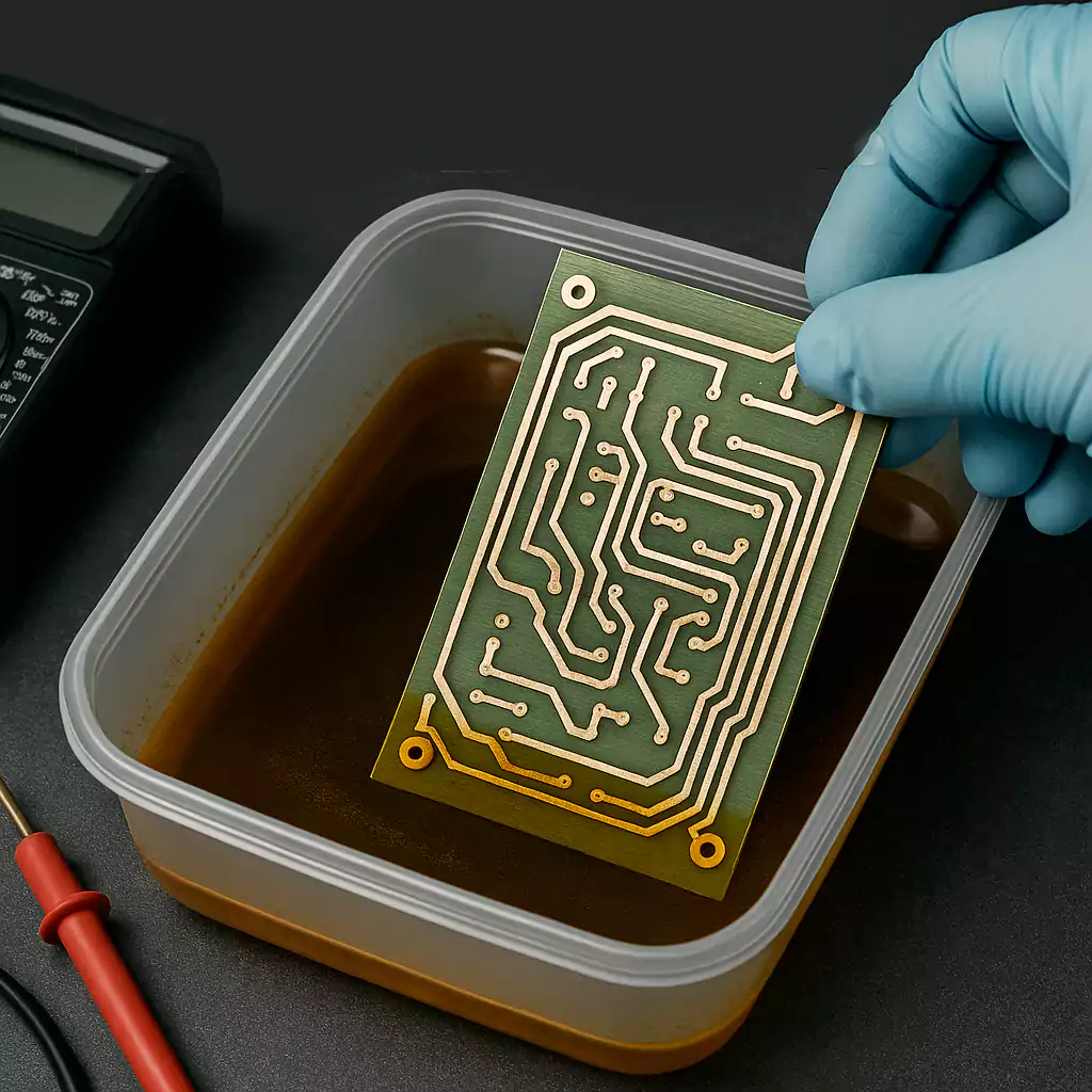
DIY PCB Etching Methods
DIY etching is commonly used for prototyping, education, or small-batch production. It relies on basic tools, household materials, and manual processes.
1.Common DIY Techniques:
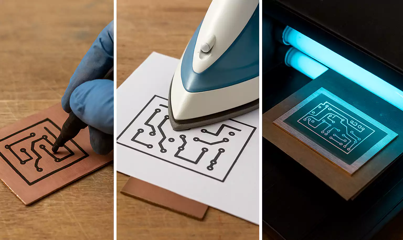
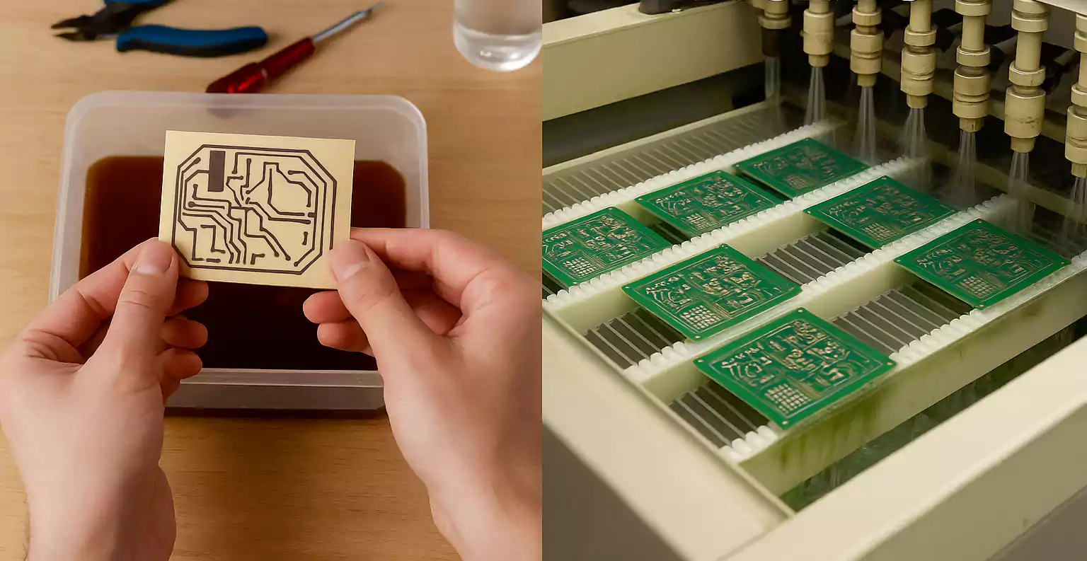
- Toner Transfer Method
A printed circuit design is transferred from glossy paper to a copper board using a household iron or laminator. After transferring, the board is etched using a chemical solution. - Permanent Marker or Hand-Drawn Method
Traces are drawn directly onto the copper board using a waterproof marker. This approach is simple but lacks accuracy for complex layouts. - Photoresist Film Method
A light-sensitive film is laminated onto the board and exposed to UV light through a printed mask. After developing the resist, the exposed copper is etched away. This method provides higher resolution and cleaner results than toner or marker-based approaches.
2.DIY Etchants:
- Ferric Chloride (FeCl₃) – Most widely used due to its effectiveness and availability.
- Cupric Chloride (CuCl₂) – Regenerable and cleaner, but requires more control.
- Hydrogen Peroxide + Hydrochloric Acid (H₂O₂ + HCl) – A powerful but hazardous option often used by advanced hobbyists.
DIY methods are affordable and flexible, but they require careful handling of chemicals and tend to have lower precision compared to industrial processes.
Industrial PCB Etching Techniques
Industrial etching is optimized for consistency, yield, and fine-line resolution. It is integrated into automated manufacturing lines and suited for complex multilayer PCBs, HDI designs, and RF/microwave applications.
1.Wet Chemical Etching
- Acidic Etching (FeCl₃ or CuCl₂)
Most commonly used for outer layers. Copper is removed using a spray or conveyor-based etching system. - Alkaline Etching
Used for inner layers of multilayer PCBs, typically employing ammonia-based etchants. Offers faster etching rates and better line edge definition.
2.Dry Etching
- Plasma Etching
A dry, gas-based process that removes copper using ionized gas. Ideal for very fine traces and high-frequency boards. - Laser Direct Imaging (LDI) + Etch
High-precision imaging combined with chemical etching. Eliminates the need for phototools and improves alignment accuracy in high-density designs.
Industrial processes are tightly controlled and scalable, offering excellent repeatability and trace fidelity, but require significant investment in equipment and environmental controls.
DIY vs. Industrial PCB Etching: Side-by-Side Comparison
Choosing between DIY etching and industrial techniques depends on your project scope, budget, and quality requirements. The following table highlights the key differences:
| Criteria | DIY Etching | Industrial Etching |
|---|---|---|
| Cost | Low (basic chemicals and tools) | High (requires advanced machinery and automation) |
| Setup Time | Quick for small jobs | Longer due to process calibration and equipment setup |
| Precision & Resolution | Moderate (limited by manual processes) | High (suitable for fine traces and HDI boards) |
| Scalability | Limited to small batches or prototypes | Scalable for high-volume production |
| Required Equipment | Minimal (iron, UV lamp, etchant container) | Specialized (etching machines, conveyors, LDI, environmental control) |
| Safety | Requires manual chemical handling; higher personal risk | Industrial safety standards; chemical exposure is contained |
| Waste Disposal | DIY users must manage chemical disposal responsibly | Managed via industrial filtration and waste treatment systems |
| Environmental Impact | Higher if chemicals are not disposed of properly | Lower due to regulatory compliance and waste management |
| Learning Curve | Beginner-friendly; ideal for education and experimentation | Requires technical training and factory integration |
| Applications | Prototyping, DIY electronics, educational use | Commercial PCBs, multilayer boards, RF and high-speed applications |
Practical Tips and Safety Guidelines
Whether you're etching PCBs at home or in an industrial facility, proper technique and safety practices are critical. Etching involves hazardous chemicals and precision-sensitive steps that can directly affect the quality, consistency, and safety of the final product.
For DIY PCB Etching
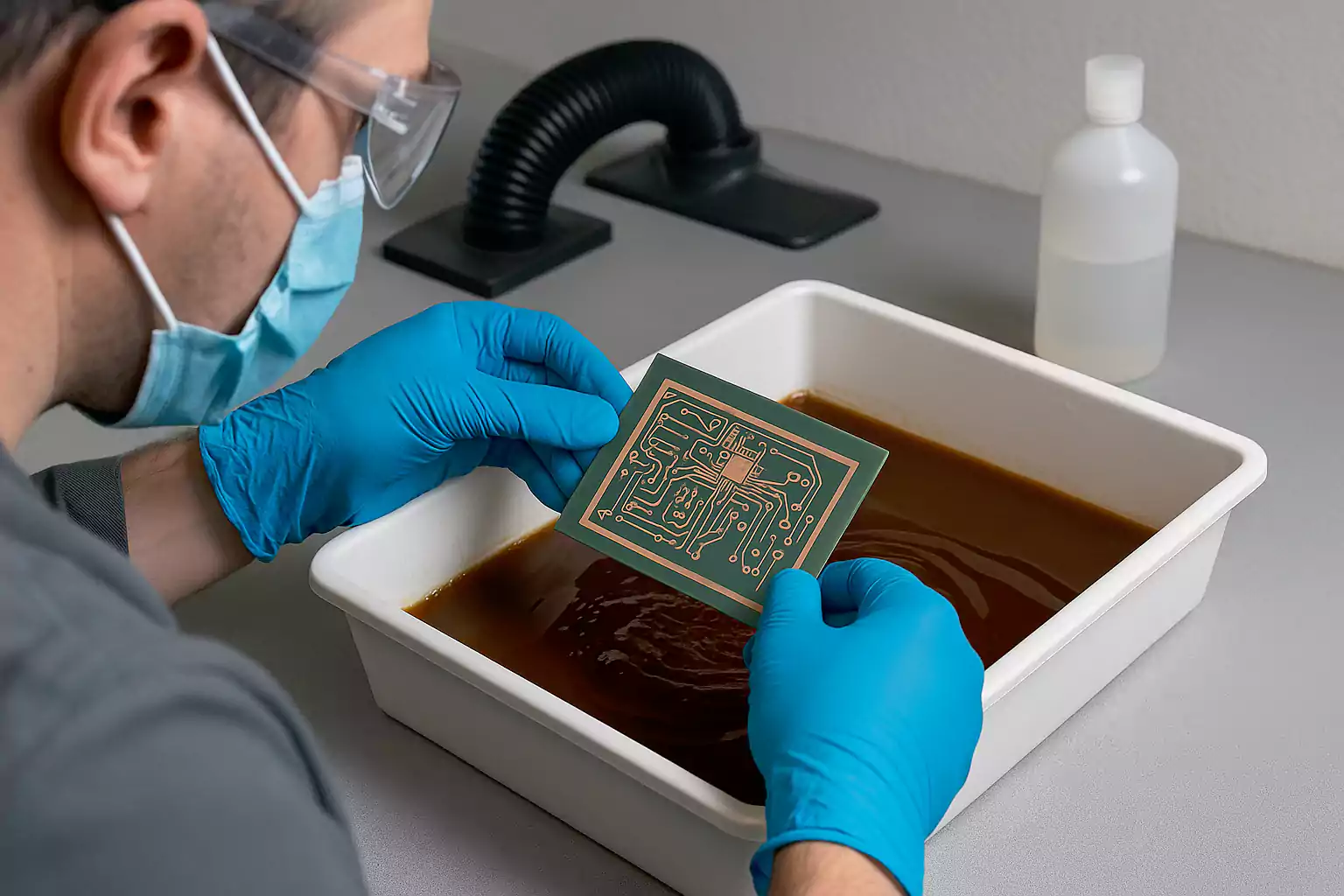
1. Use Proper Personal Protective Equipment (PPE)
Always wear gloves, safety goggles, and a lab apron when handling etchants like ferric chloride or hydrogen peroxide + hydrochloric acid mixtures. These chemicals can stain skin, cause burns, or release toxic fumes.
2. Ensure Good Ventilation
Work in a well-ventilated area or under a fume hood. Some DIY mixtures release chlorine gas or acidic vapors, especially when heated.
3. Label and Store Chemicals Carefully
Use sealed, clearly labeled containers. Avoid cross-contamination and keep acids out of reach of children and pets.
4. Avoid Over-Etching
Monitor etching progress regularly. Over-etching can lead to thin traces, loss of conductivity, or damaged pads. Agitate the solution gently for even etching.
5. Responsible Waste Disposal
Never pour used etchant down the drain. Neutralize the solution (e.g., with baking soda for acid-based mixtures) and follow local hazardous waste disposal guidelines.
For Industrial PCB Etching
1. Monitor Chemical Concentration
Regularly test etchant strength (Baumé reading or pH level) to ensure optimal performance and consistency across batches.
2. Calibrate Spray Systems and Conveyor Speed
Precise timing and uniform spray coverage are essential for even etching and avoiding under- or over-etched areas.
3. Implement Closed-Loop Filtration Systems
Recycling etchant and managing waste through proper filtration reduces costs and environmental impact.
4. Train Operators on Safety Protocols
Ensure all personnel are trained on emergency handling procedures, PPE use, and chemical spill response.
5. Maintain Equipment Regularly
Etching machines should be inspected for nozzle clogs, leaks, and pump wear to avoid unplanned downtime and quality issues.
Trends and Future Outlook
The PCB etching process is evolving alongside advances in electronics manufacturing. As designs become more compact and performance-driven, etching techniques are adapting to meet higher precision, environmental, and automation demands.
High-Density and Microvia Designs
The shift toward HDI (High-Density Interconnect) PCBs and microvias requires finer trace widths and tighter tolerances. This trend is pushing the development of more accurate etching systems, especially in dry etching and laser-assisted methods.
Environmentally Safer Etchants
To address environmental concerns, manufacturers are exploring non-toxic etching solutions, such as regenerable cupric chloride systems and ferric-based closed-loop setups. Regulatory pressure is accelerating the shift toward sustainable chemical handling and waste treatment.
Laser Direct Imaging (LDI) Integration
LDI is gaining traction as a maskless imaging method that improves alignment precision and reduces defects. When paired with high-speed etching systems, it enables faster prototyping and fine-line production.
Automation and Smart Process Control
Modern etching lines are integrating real-time monitoring, AI-based parameter adjustment, and predictive maintenance to reduce human error and increase throughput. This is particularly valuable in multi-layer and high-volume PCB production.
Additive Alternatives
While subtractive etching remains dominant, additive manufacturing methods such as inkjet-printed circuitry or 3D copper deposition are being researched as cleaner, faster alternatives for specific applications.
User Recommendation Guide
Selecting the right PCB etching method depends on your role, production goals, and resource availability. This guide outlines practical recommendations based on common user scenarios.
For Hobbyists & DIY Makers
If you're building simple circuits or learning PCB fabrication:
- Recommended Method: Toner transfer or photoresist film + ferric chloride or cupric chloride.
- Why: Low cost, accessible tools, and hands-on learning. Ideal for prototypes and small projects.
- Tip: Use pre-sensitized boards for better consistency and cleaner traces.
For Engineering Students & Educators
If you're teaching or experimenting with PCB processes:
- Recommended Method: UV photoresist exposure with controlled etchant handling.
- Why: Balances safety, accuracy, and process visibility for learning environments.
- Tip: Integrate a full design-to-fabrication workflow to reinforce engineering principles.
For Small-Scale Startups & R&D Labs
If you're producing early-stage hardware or custom boards:
- Recommended Method: LDI-based photoimaging with closed-loop wet etching systems.
- Why: Offers finer resolution and reproducible results without full-scale industrial infrastructure.
- Tip: Outsource complex multilayer boards but retain in-house capacity for rapid single-layer prototyping.
For Industrial Manufacturers
If you manage mass production or multilayer PCB lines:
- Recommended Method: Automated alkaline or acid etching lines with inline monitoring and waste treatment.
- Why: Ensures high throughput, consistency, and regulatory compliance.
- Tip: Integrate real-time process analytics to reduce defects and optimize material usage.
For Sustainability-Focused Teams
If your priority is minimizing environmental impact:
- Recommended Method: Regenerative cupric chloride systems or explore additive PCB technologies.
- Why: Reduced hazardous waste and potential for lower lifecycle cost.
- Tip: Evaluate total environmental footprint, including energy use and effluent disposal.
Conclusion
PCB etching plays a decisive role in defining circuit accuracy and production quality. From accessible DIY methods to advanced industrial systems, each approach serves a specific purpose based on scale, precision, and resource requirements.
As manufacturing evolves, trends like high-density layouts, sustainable etching solutions, and process automation are shaping the future of PCB fabrication. Choosing the right method ensures both technical reliability and process efficiency.
Understanding your needs—and aligning them with the appropriate etching strategy—is key to successful PCB development.