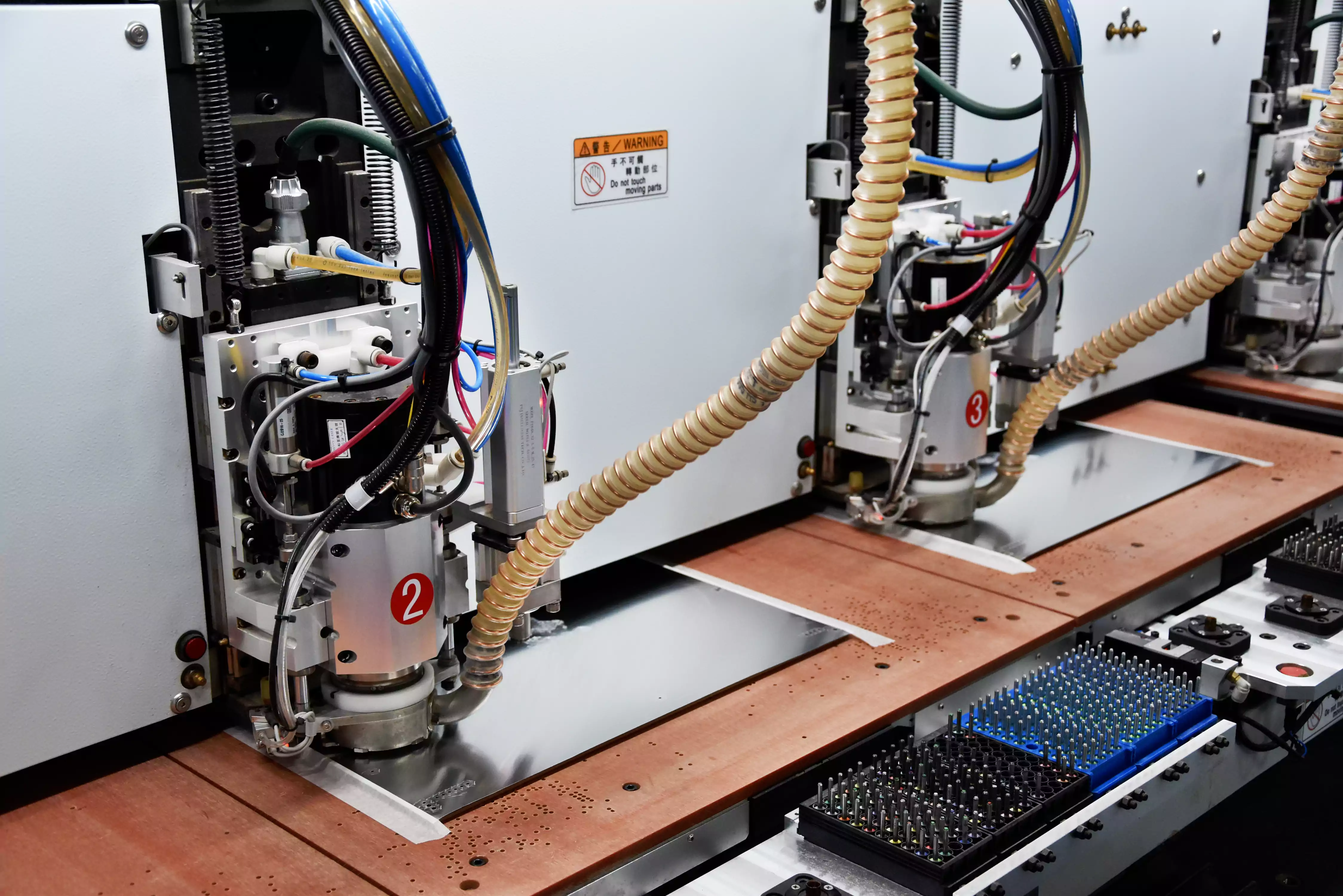
PCB drilling is one of the most critical processes in printed circuit board manufacturing. PCB Drilling Quality directly affects downstream processes such as electroless copper deposition, plating, imaging, and interlayer interconnection. It also has a major impact on PCB hole quality, electrical performance, mechanical reliability, and the long-term durability of the finished board.
As a result, using the appropriate evaluation methods for drilled holes is essential for both process control and quality assurance in PCB fabrication.
This article explains eight key inspection criteria commonly used to evaluate PCB drilling quality and identify common PCB drilling defects:
- Drill hole diameter
- Hole position accuracy
- Hole wall roughness
- Burrs
- Nail heading
- Wicking
- Haloing
- Plugged holes
Drill Hole Diameter
1. What is the drill hole diameter?
Drill hole diameter refers to the hole diameter immediately after it is mechanically drilled into a single-sided, double-sided, or multilayer PCB panel. At this stage, the hole has not yet been metallized, so there is no conductive layer on the hole wall.
This differs from the finished hole size, which refers to the final hole diameter of the completed PCB. For plated through-holes, copper and other metallized layers are deposited on the hole wall during subsequent processes, so the finished hole size is smaller than the original drill hole diameter. This dimensional relationship is a basic part of PCB hole quality inspection.
2. Common inspection methods
Typical tools and methods used to check drill hole diameter include:
- Pin gauges
- Vision measuring systems
- Hole inspection machines
- Horizontal cross-section analysis
3. Typical acceptance standard
A common evaluation standard for drill hole diameter is:
D ± 0.025 mm
where D is the target drill diameter.
Actual tolerances may vary depending on the PCB manufacturer’s internal control standards and customer requirements.
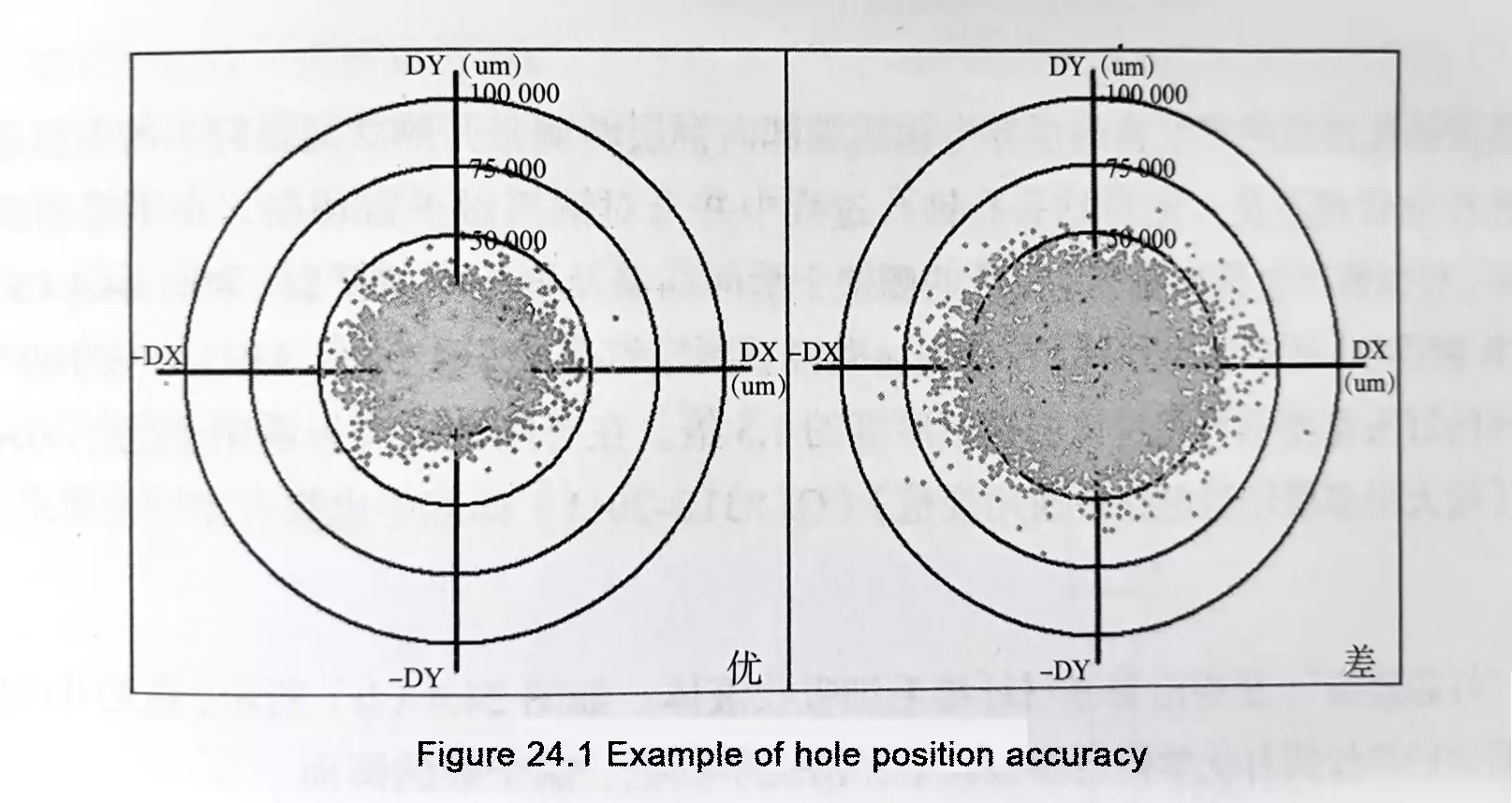
Hole Position Accuracy
1. What is the hole position accuracy?
PCB hole position accuracy describes how closely the actual drilled hole location matches the intended design location. It is one of the most important indicators of drilling precision and overall PCB Drilling Quality.
Poor hole position accuracy can lead to:
- Off-center holes
- Reduced annular ring
- Inner-layer breakout
- Unreliable interlayer connection
- Lower final yield
2. Cpk as the main evaluation metric
In the PCB industry, hole position accuracy is commonly measured using the process capability index, typically expressed as Cpk or Cp.
Cpk reflects the actual manufacturing capability of a process when it is operating in a stable, controlled state over time. In other words, it indicates how consistently the drilling process meets the required quality standard.
This capability is influenced by the combined effect of five major quality factors:
- Operator
- Machine
- Raw materials
- Process method
- Production environment
A higher Cpk means the drilling process is more stable and better able to maintain PCB hole position accuracy.
3. Common inspection methods
Hole position accuracy is typically measured using:
- Hole position inspection machines
For qualitative checks, such as determining whether hole shift exists, manufacturers may also use:
- Red film
- Dot maps
4. Typical industry requirement
In PCB manufacturing, a common requirement is:
Cpk ≥ 1.33 (±3 mil)
This indicates that the drilling process should have sufficient stability and production capability.
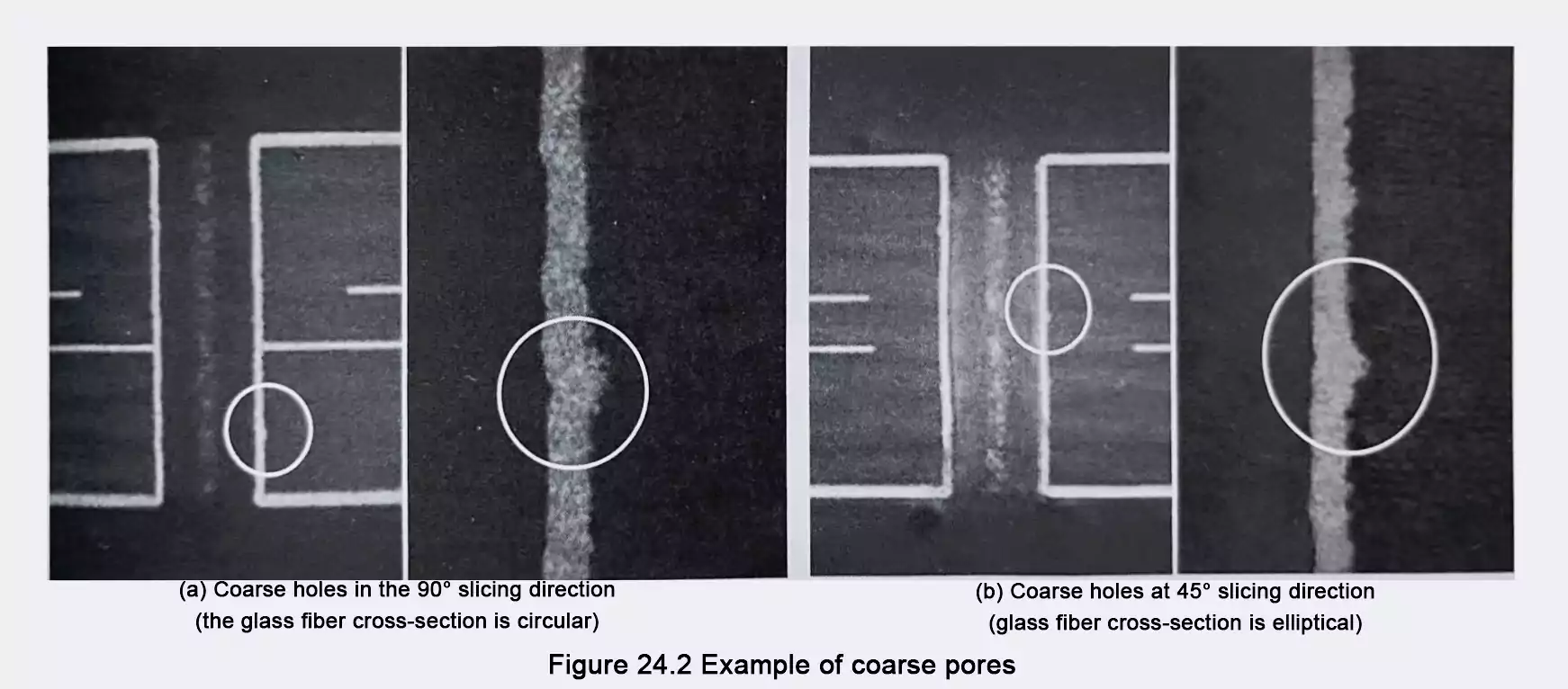
Hole Wall Roughness
1. What is the hole wall roughness?
Hole wall roughness in PCB drilling refers to the unevenness of the hole wall resulting from cutting and friction during drilling.
Excessive hole wall roughness PCB defects can create several risks:
- Poor electroless copper coverage
- Weak plating adhesion
- Higher risk of hole wall defects
- Reduced reliability of plated interconnections
2. Why cross-section direction matters
Because PCB laminates contain woven glass fiber, the direction in which a hole is cross-sectioned has a major influence on the observed roughness. Two common cross-section directions are:
- 90° to the glass weave
- 45° to the glass weave
In practice, hole roughness seen in a 45° cross-section is usually much greater than what is seen in a 90° cross-section.
For that reason, the industry’s default inspection direction is generally:
90° to the glass weave
3. Typical control standard
A commonly used internal control target is:
Less than 30 μm
In addition, IPC-DR-572A, Printed Board Drilling Guide, recommends controlling hole roughness to:
Less than 25 μm
However, that guideline does not specify:
- The cross-section direction used for measurement
- The hole diameter being evaluated
4. Practical considerations
In real production, it can be difficult to keep roughness below 25 μm under conditions such as:
- Hole diameters above 1.0 mm
- PCB constructions using multiple plies of 7628 glass cloth
- Cross-sectioning at 45° to the glass weave
For this reason, PCB manufacturers are generally advised to define acceptable standards based on actual product structure and process capability, then align those criteria with the end customer.
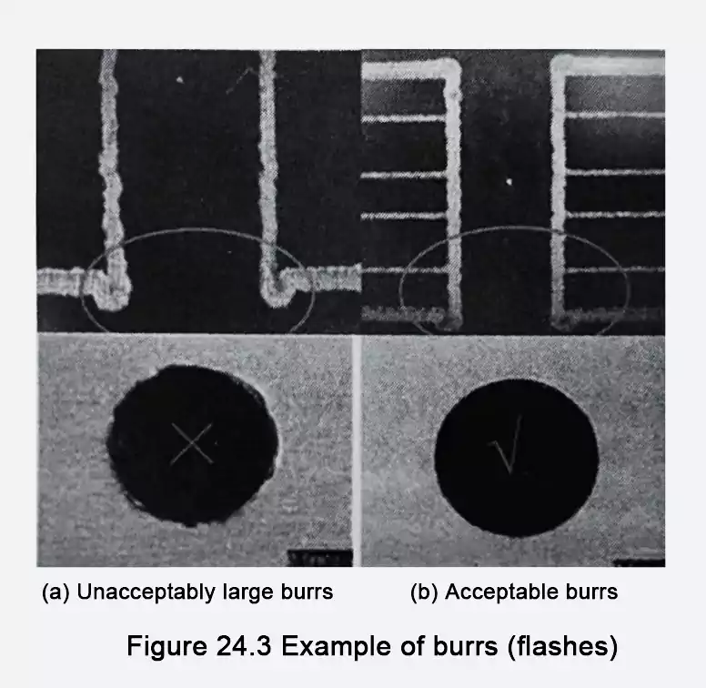
Burrs
1. What are burrs?
A burr is a raised edge or protrusion formed when the copper foil on the board surface is stretched during drilling and is not completely cut off. Because copper is ductile, it can deform rather than break cleanly during drilling.
If burrs are not removed, they may become larger protrusions after electroless copper plating, affecting both appearance and reliability. This is one of the more common PCB drilling defects seen in mechanical drilling.
2. Where burrs usually occur
Burrs are commonly found at:
- The entry side of the panel
- The exit side of the backup board
3. Main causes of burrs
The most common causes include:
- Insufficient support from the entry or backup material
- Dull drill bits
- Excessive hits per drill bit
4. Recommended acceptance criteria
For burr height, the commonly recommended limits are:
- For hole diameters ≤ 1.25 mm, the maximum acceptable burr height is 1% of the drill diameter
- For hole diameters > 1.25 mm, the maximum acceptable burr height is 12 μm
Nail Heading
1. What is nail heading?
PCB nail heading is a condition in multilayer PCBs in which the ends of the inner-layer conductive copper foil are forced outward on both sides during drilling.
This is essentially a mechanical deformation of the inner-layer copper caused by abnormal drilling conditions and is an important defect in evaluating the quality of plated-through holes in multilayer boards.
2. How nail heading forms
Nail heading is usually caused by:
- Worn drill bits
- Poor drilling process control
When a dull drill bit passes through copper foil, it may no longer cut the copper cleanly. Instead, it pushes the copper to the side under high temperature and pressure. As a result, the sidewall of the inner-layer annular ring becomes flattened and spreads outward, producing the nail head shape.
3. Inspection method
In PCB manufacturing, nail heading is typically evaluated by:
- Preparing cross-sections
- Observing the whole structure under a metallographic microscope
4. Acceptance criteria
For example, MIL-P-55110E specifies that:
The nail head width of the inner-layer land in a multilayer board must not exceed 1.5 times the thickness of that copper foil layer.
The same requirement also appears in:
- GJB362B-2009, General Specification for Rigid Printed Boards
- QJ831B-2011, General Specification for Multilayer Printed Circuit Boards for Aerospace Use
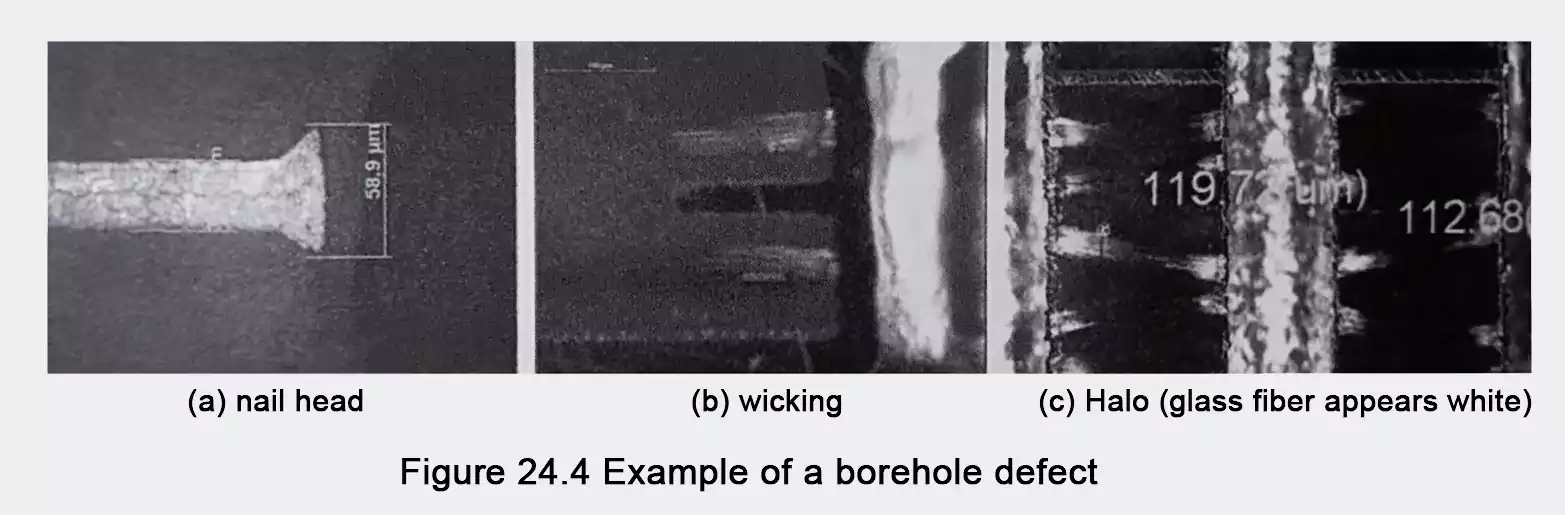
Wicking
1. What is wicking?
Wicking in PCB holes, also known as the wick effect, refers to capillary absorption of liquid along the substrate fibers.
In a hole wall cross-section, when electroless copper penetrates the spaces between individual filaments in the exposed glass fiber bundles, the microstructure may appear as a broom or brush pattern. That appearance is considered evidence of wicking.
2. What wicking indicates
Wicking suggests that the fiber structure along the hole wall has been exposed, allowing process chemicals and deposited copper to penetrate into the glass bundle.
This can affect the whole wall interface condition and is often an important concern in high-reliability PCB applications.
Haloing
1. What is haloing?
PCB haloing, also called a white ring, is a condition in which mechanical processing causes fractures or separations within the substrate, either on the surface or below it.
It typically appears as whitening around a drilled hole or around another machined feature.
2. How haloing forms
Haloing is caused by mechanical stress damage to the laminate. During drilling or other machining operations, excessive cutting force, friction, or poor processing conditions can damage the resin-to-glass interface, creating a visibly whitened region.
3. Acceptance requirement
The halo penetration distance must not exceed:
- 2.5 mm, or
- 50% of the distance to the nearest conductor
Haloing is more than just an appearance issue. It can indicate structural damage in the base material, making it especially important for high-reliability PCB products.
Plugged Holes
1. What are plugged holes?
During PCB drilling, if chips cannot be removed effectively, they may become trapped in the hole, creating a plugged hole condition.
This is another important item in PCB drilled hole inspection criteria.
2. Main causes of plugged holes
Plugged holes are commonly caused by:
- Insufficient chip evacuation space in the drill bit
- Inadequate vacuum or dust collection
- Excessive board thickness
- Poor chip removal during drilling
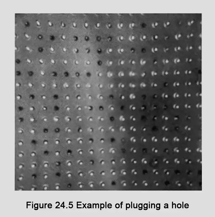
3. Why plugged holes matter
Plugged holes can seriously affect downstream processing, including:
- Abnormal hole wall condition
- Poor electroless copper coverage
- Poor plating quality
- Foreign material left inside the hole
- Reduced interconnection reliability
Because of this, plugged holes are a critical defect that must be controlled during drilling.
Why PCB Drilling Quality Evaluation Matters
As these eight criteria show, PCB Drilling Quality cannot be judged simply by whether a hole was successfully drilled. It must be evaluated from multiple perspectives, including size, location, hole wall condition, copper deformation, substrate damage, and chip evacuation.
These PCB drilled hole inspection criteria are important for several reasons.
1. They help ensure stable downstream processing
Drilling quality directly affects:
- Electroless copper deposition
- Electroplating
- Imaging
- Lamination alignment
- Routing and profiling
- Electrical testing
If hole quality is unstable during drilling, downstream yield becomes much harder to control.
2. They improve electrical interconnection reliability
For multilayer boards and plated-through holes in particular, issues such as hole wall roughness, nail heading, and wicking are closely tied to the long-term reliability of interlayer electrical connections and to overall plated-through-hole quality.
3. They reduce batch defect risk
By defining clear standards for hole diameter, PCB hole position accuracy, burrs, haloing, and other PCB drilling defects, manufacturers can build a more stable process control system and reduce the risk of large-scale production issues.
4. They help align standards between the PCB factory and the customer
Some items, such as hole roughness and haloing, can vary depending on material construction, hole size, and cross-section direction. For that reason, agreeing on practical acceptance standards with the end customer is often necessary for efficient quality communication.
Conclusion
PCB drilling may look like a basic fabrication step, but it is one of the most important processes in PCB manufacturing. From drill hole diameter and PCB hole position accuracy to hole wall roughness, PCB defects, burrs, nail heading, wicking, haloing, and plugged holes, every evaluation item corresponds to a specific process risk and potential reliability concern.
For PCB manufacturers, the key to improving PCB Drilling Quality is to establish a complete evaluation system and combine it with proper control of equipment condition, drill bit life, laminate structure, and customer requirements. Only then can they improve process consistency, final yield, PCB hole quality, and long-term reliability.