


Many PCBs “work electrically” but still fail in production because the layout ignored PCB DFM (Design for Manufacturability) and DFT (Design for Test). The result is predictable: SMT line alarms, unstable handling, poor solder joints, higher rework, and weak test coverage.
Below is a shop-floor-focused guide to the most common PCB design mistakes, the SMT defects they trigger, and the DFM rules that prevent them—covering PCB panelization, fiducial marks, tooling holes, tombstoning, via-in-pad, ICT test points, and solder mask.

1. Missing Tooling Holes and Process Rails: A “Non-Runnable” PCB
PCB design mistake: No tooling holes and no process rails (panel rails / break-away edges).
DFM impact: SMT equipment can’t consistently clamp or align the board.
What you’ll see on the line:
- Solder paste printer misalignment.
- Pick-and-place vision/placement errors
- Conveyor instability, board skew, frequent alarms
DFM fix:
- Add panel rails and standardized tooling holes for registration and handling.
- Ensure the assembly house’s minimum rail width and hole specs are met.
2. Extreme Board Size or Irregular Outline: Handling and Placement Instability
PCB design mistake: Board is too small/too large or overly irregular.
DFM impact: Doesn’t fit the SMT line’s mechanical window or needs costly fixtures.
Common outcomes:
- Poor conveyance (tilting, vibration)
- Placement drift and print defects
- Higher warpage risk during reflow
DFM fix:
- Use PCB panelization with rails to stabilize the assembly size.
- Avoid outlines that standard conveyors can’t support
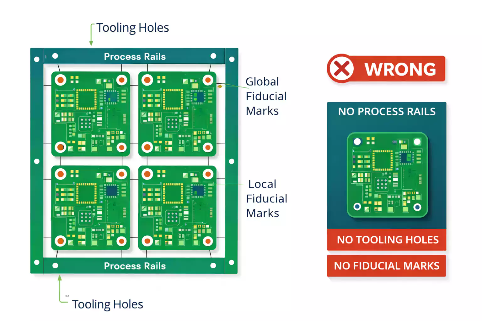
3. Fiducial Marks Done Wrong: Vision Errors and Placement Alarms
PCB design mistake: Missing or non-standard fiducial marks (Mark points), especially near fine-pitch ICs (like FQFP).
Common fiducial problems include:
- Solder mask too close or covering the copper
- Wrong fiducial size (too big/too small)
- Poor contrast area around the fiducial
What happens:
- Pick-and-place cameras can’t reliably lock onto the fiducial.
- Frequent machine alarms and placement accuracy issues
DFM fix:
- Use standard global + local fiducials.
- Keep fiducials clean (no mask/legend interference) with proper clearance for contrast.
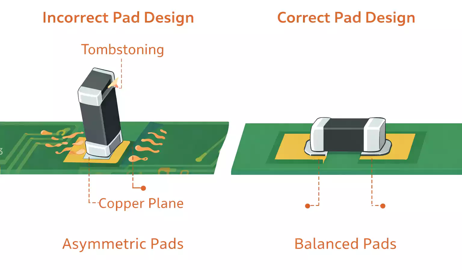
4. Wrong SMT Pad Geometry: Skew, Rotation, and Tombstoning
PCB design mistake: Incorrect pad size/spacing for chip components, or asymmetric pads.
SMT defects: Misalignment, skew, and tombstoning.
Why it happens (reflow dynamics):
During reflow, solder paste melts, and surface tension forces act on the component. If pads are unbalanced, those forces become unbalanced too—components shift or lift.
DFM fix:
- Use proven IPC-style footprints or manufacturer land patterns.
- Keep pad geometry symmetrical (size, shape, solder paste volume)
5. Via-in-Pad Without Proper Processing: Solder Starvation
PCB design mistake: Via-in-pad with open vias (not filled/plugged).
SMT defects: Low solder volume, weak joints, intermittent opens.
What happens:
Molten solder wicks down the via during reflow, leaving insufficient solder at the pad.
DFM fix:
- Avoid via-in-pad unless necessary.
- If required, specify proper via treatment (filled/plugged and planarized per your fab/EMS capability)
6. Ground Copper Used as a Pad: Thermal Imbalance → Tombstoning
PCB design mistake: One pad is tied into a large ground area or trace-as-pad, while the other pad is smaller.
SMT defects: Tombstoning (especially on small passives).
Why does it happen:
Large copper = higher thermal mass = slower heating. One side melts later, and surface tension pulls the part upright.
DFM fix:
- Balance copper around pads
- Use thermal reliefs where appropriate.
- Keep both terminations thermally similar.
7. Fine-Pitch IC Pads Too Wide or Too Short: Bridging and Weak Joints
PCB design mistake (FQFP example):
- Pads too wide → solder accumulates → bridging.
- Pad heel/toe too short → reduced joint strength
SMT defects:
- Solder bridging (shorts)
- Fragile joints, poor reliability
DFM fix:
- Follow validated land patterns for fine-pitch packages.
- Tune pad width/length and solder mask strategy for your process window
8. Routing Between Pads in the Middle: Harder AOI / Visual Inspection
PCB design mistake: Interconnect traces placed centrally between fine-pitch pads.
Impact: Worse inspection visibility after reflow.
What happens:
AOI and manual inspection struggle to see true solder fillet edges—bridges and insufficient solder are easier to miss.
DFM fix:
- Route to preserve solder joint visibility where possible
- Don’t trade inspection margin for minor routing convenience.
9. Wave Solder Designs Without Helper Features: Bridging Risk
PCB design mistake: Wave-soldered ICs lack auxiliary pads / solder-thieving features.
SMT defect (wave): Bridging after wave solder.
DFM fix:
- Design for the wave direction and solder flow
- Add appropriate helper features (as supported by your assembler)
10. Poor Component Distribution: Reflow Warpage and Post-Solder Deformation
PCB design mistake: ICs concentrated in one area; copper and mass distribution unbalanced.
Impact: PCB warpage after reflow, second-side assembly instability.
SMT defects and consequences:
- Placement shift
- Stress on fine-pitch/BGA joints
- Fixture/test fit problems
DFM fix:
- Balance copper distribution
- Avoid heavy component clustering without mechanical consideration.
- Consider the stack-up and panel support strategy early.
11. ICT Test Points Not DFM-Friendly: Low Coverage or No Test
PCB design mistake: ICT test points are missing, too small, inaccessible, or too close together.
Impact: ICT can’t probe reliably—or can’t run at all.
DFM/DFT fix:
- Provide accessible, properly spaced test points on critical nets.
- Avoid placing test points under components or in keep-out regions.
12. Insufficient Spacing Between SMDs: Rework Becomes Risky
PCB design mistake: SMD-to-SMD clearance too tight.
Impact: Rework is slow, risky, and sometimes impossible.
DFM fix:
- Keep practical rework clearance for hot air nozzles and irons.
- Treat repairability as part of manufacturability.
13. Solder Mask and Silkscreen Over Pads: Non-Wet Opens and Intermittents
PCB design mistake: Poor solder mask openings or silkscreen printed onto pads.
SMT defects: Poor wetting, cold joints, opens, intermittent failures.
DFM fix:
- Enforce solder mask clearance rules.
- Keep silkscreen out of solderable areas.
- Verify mask expansion and registration tolerances.
14. Bad PCB Panelization or V-Score Design: Warpage After Reflow
PCB design mistake: PCB panelization or V-score strategy is poorly designed or poorly manufactured.
Impact: Warpage after reflow, stress during depaneling.
Common issues:
- Weak panel tabs or uneven support
- V-score depth/location not matched to board thickness and layout.
DFM fix:
- Use panel rails + stable tab/V-score strategy.
- Place break points away from sensitive components and fine-pitch joints
Root Causes: Why These PCB Design Mistakes Keep Happening
Most failures trace back to three realities:
- Designers underestimate reflow as a dynamic process
SMT defects like tombstoning and skew aren’t random—they’re physics + footprint + thermal balance. - Process engineers aren’t involved early enough.
PCB DFM and assembly constraints are often discovered only during pilot runs. - No consistent internal PCB DFM / DFT guidelines
Without standard rules for footprints, fiducials, tooling holes, panelization, ICT test points, and solder mask, every project reinvents (and repeats) the same mistakes.
Practical Takeaway: A DFM Mindset Prevents Most SMT Defects
If you want fewer SMT defects and smoother production, treat PCB layout as part of the manufacturing system:
- PCB DFM: tooling holes, panel rails, fiducial marks, panelization strategy, copper balance
- SMT reliability: pad symmetry, via-in-pad control, thermal balance to prevent tombstoning
- DFT: ICT test points with good access and spacing
- Process hygiene: clean solder mask openings and silkscreen keep-outs