If you’re designing a board that needs to build cleanly, pass EMI, and behave consistently in real hardware, you can’t treat layout as an afterthought. Strong PCB design rules—especially around placement, routing, and copper geometry—are what turn a correct schematic into a reliable product.
This article is a practical set of PCB Design Rules focused on three foundations: PCB component placement, PCB routing rules, and trace width and spacing.
1. PCB Component Placement Rules
PCB component placement means arranging parts based on the schematic’s functional intent and each package’s physical dimensions. Placement quality affects assembly yield, debug/repair effort, and final electrical performance.
Follow these PCB design rules for placement:
(1) Keep placement even; group parts by function
- Distribute components evenly and neatly.
- Keep parts within the same functional block, and keep them relatively close together for easier testing, debugging, and service.
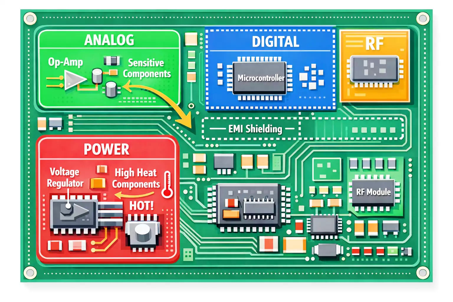
(2) Place electrically connected parts close to reduce routing length
- Components that connect should be placed nearby.
- Shorter connections improve routing density and help minimize parasitics.
(3) Separate heat-sensitive components from heat sources
- Keep temperature-sensitive parts away from high-power devices and other major heat generators to reduce drift and improve stability.
(4) Isolate or shield components that may cause EMI issues
- For parts that are likely to interfere electromagnetically, use spacing, shielding, or isolation as needed.
2. PCB Routing Rules
Routing is where PCB design rules become real copper. Good routing reduces noise, limits coupling, and improves manufacturability.
(1) Choose layers in this order: single → double → multilayer
As long as requirements are met, prefer simpler stackups first:
- Single-layer, then two-layer, then multilayer routing.
(2) Keep traces short; route sensitive/small signals first
- Keep traces between pads as short as possible.
- Route sensitive and small signals first to reduce delay and interference.
- In analog sections, route a ground trace alongside input traces for shielding where appropriate.
- Keep routing on the same layer evenly distributed and try to balance the copper area to reduce warpage risk.
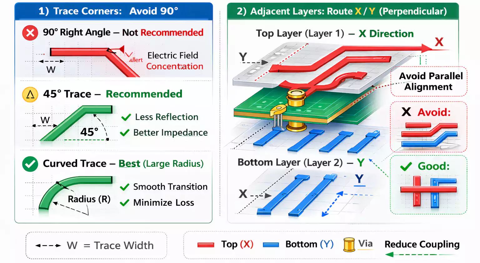
(3) Avoid sharp corners: use 45° bends or smooth arcs
- Direction changes should use 45° angles or smooth curves with larger radii.
- This helps avoid field concentration, reflections, and extra impedance discontinuities.
(4) Separate digital and analog routing—and separate their power/ground systems
- Route digital and analog sections separately to prevent mutual interference.
- If they share a layer, keep their power distribution and ground distribution routed separately.
- For signals at different frequencies, consider a ground trace between them to reduce crosstalk.
(5) Keep power and ground connections short and close
- Short, closed power/ground routing reduces internal resistance.
(6) Route adjacent layers orthogonally (X/Y); avoid parallel overlap
- Use perpendicular routing directions on adjacent layers to reduce coupling.
- Avoid long parallel runs, and avoid aligning traces directly above/below each other.
(7) Length-match critical high-speed I/O and balanced/differential paths
- High-speed multi-I/O and balanced/differential-related I/O paths should be of equal length to prevent unwanted delay or phase shift.
(8) Use thermal relief for pads tied to large copper—except >5 A pads
For pads connected to large copper areas, apply thermal relief:
- Spoke length ≥ 0.5 mm
- Spoke width ≥ 0.13 mm
- Do not use thermal relief for pads carrying more than 5 A.
(9) Maintain trace-to-edge clearance
- The closest traces should generally be > 5 mm from the PCB edge.
- Ground traces may be allowed closer when necessary.
- If the board slides into rails/guides, keep clearance greater than the guide slot depth.
(10) Design power and ground for low impedance (2-layer and multilayer)
- On two-layer boards, place the common power and ground near the edge and, when possible, distribute them on both sides to achieve low impedance.
- On multilayer boards, use dedicated power/ground planes and connect with plated-through vias.
- Inner-layer large copper (power/ground) can use a mesh pattern to improve interlayer bonding strength.
(11) Add breakpoints and test points for easier testing
- Include required breakpoints and test points to simplify validation and production testing.
3. Trace Width and Spacing
Trace width depends on load current, allowable temperature rise, and practical manufacturing limits (including copper adhesion). In general:
- Typical traces are at least 0.2 mm wide, often with a copper thickness of≥ 18 μm.
- SMT and high-density boards may use thinner traces, but finer geometry increases manufacturing difficulty—choose wider traces when space allows.
(1) Keep signal trace widths consistent; make power/ground wide
- Consistent signal widths help with impedance consistency and matching.
- A common signal width guideline is 0.2–0.3 mm (8–12 mil).
- Use wider copper for power/ground to reduce interference.
- For high-frequency signals, add adjacent ground shielding where appropriate.
(2) High-speed and microwave lines must meet characteristic impedance targets
- Width and thickness must be selected to meet impedance requirements.
(3) High-power designs: consider current density and insulation
- Include spacing/insulation constraints, not just width.
- Inner-layer conductors typically allow about half the current density of outer layers.
(4) Increase spacing when possible to improve insulation resistance
Surface-layer insulation resistance is influenced by:
- Trace spacing
- Parallel run length
- The insulating medium (substrate and air)
When routing space permits, increase spacing.
Final Takeaway
These PCB design rules and PCB design guidelines are simple, but they prevent a huge percentage of real-world problems:
- Start with disciplined PCB component placement.
- Apply conservative PCB routing rules for separation, coupling control, and testability.
- Use realistic trace width and spacing that support current, impedance, and manufacturing capability.