


Introduction
PCB Components Identification is one of the most valuable skills in electronics repair, design, and troubleshooting.
This practical guide will show you a simple, step-by-step process for recognizing standard electronic parts on a PCB—from resistors and capacitors to ICs, connectors, and jumpers.
We’ll explain how reference designators work, how to read polarity and pin-1 markings, and how to test parts safely.
The 30-Second PCB Check
Before diving deep, you can learn a lot just by scanning the board in three quick passes:
- Find the silkscreen reference codes. Every part has a printed ID, such as R105, C23, U7, or JP1.
- Look at the shape and markings. Package type, size, and any bands, dots, or notches reveal polarity or orientation.
- Verify with a multimeter or visual test. Check for continuity, diode direction, and obvious damage, such as burnt, cracked, or swollen parts. Mastering this pattern makes identifying most of the board intuitive.
Understanding Reference Designators
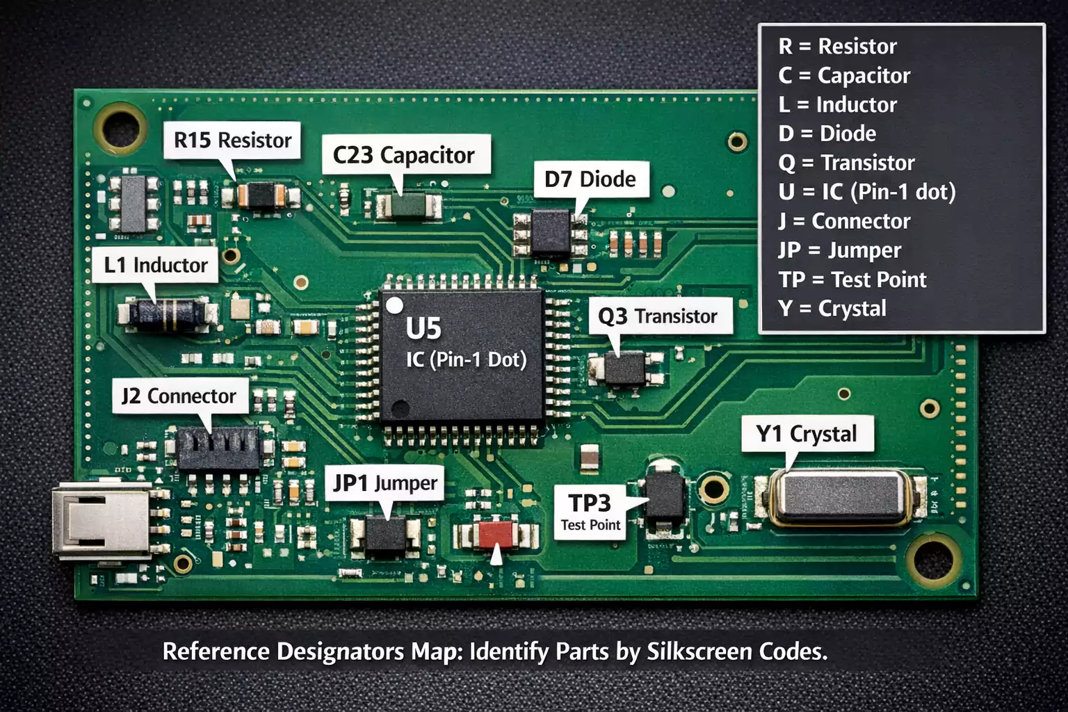
Each PCB component is labeled with a Reference Designator, a short alphanumeric code that identifies the component type and its unique location on the schematic and layout.
Designators are your m: U3 always refers to the same IC on both the schematic and the physical PCB. Cross-reference the ID in the documentationID to reveaitsct model and ecs.specs.
Visual Identification of Common Components
Recognizing components by their shape and markings is the fastest way to understand a circuit at a glance.
1. Passive Components
- Resistors (R)
Cylindrical through-hole resistors use color bands that represent numeric values (e.g., brown-black-red = 1 kΩ).
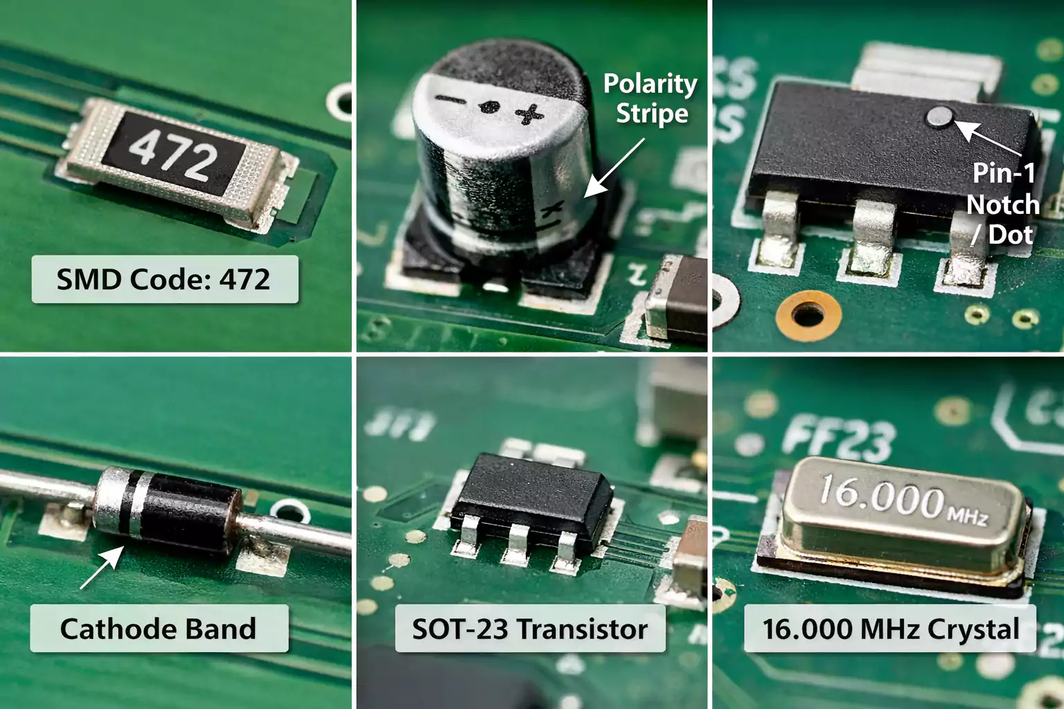
Surface-mount (SMD) resistors use three- or four-digit codes, such as 472 (4.7 kΩ).
Potentiometers, or variable resistors, often have a small knob or a slot for adjustment. - Capacitors (C)
Ceramic capacitors are tiny, brown or beige rectangles with no polarity.
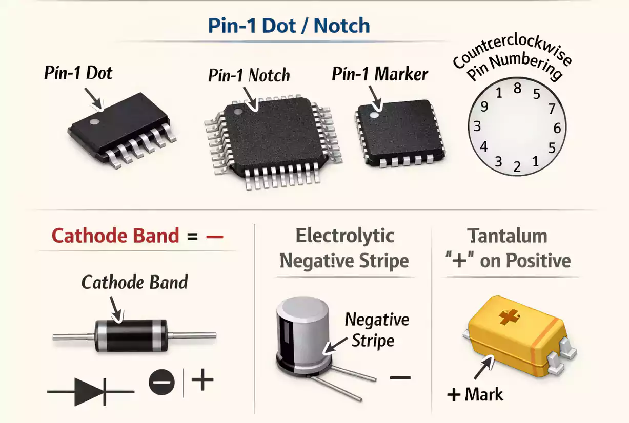
Electrolytic or tantalum capacitors are polarized—look for a stripe or “+” sign. Values and voltage ratings are printed on the can (e.g., 47 µF 25 V). V). - Inductors & Ferrite Beads (L, FB)
Often look like small black blocks or coils. Ferrite beads filter high-frequency noise and are sometimes labeled FB1 or FB2.
2. Diodes and LEDs (D)
A diode allows current to flow in only one direction. The stripe or notch marks the cathode (negative side).
Light-emitting diodes (LEDs) have one longer lead for the anode (+) and a flat edge for the cathode (–).
3. Transistors and MOSFETs (Q)
Three-terminal devices are used for switching and amplification. Small-signal transistors are in SOT-23 packages, while power MOSFETs are in TO-220 or D-PAK packages. A printed code (e.g., “A06,” “IRFZ44N”) helps you look up the part.
4. Integrated Circuits (U)
ICs are rectangular packages with multiple pins. The notch or dot marks pin 1.
Common types include voltage regulators, microcontrollers, op-amps, and logic chips. If unsure, search the part number or marking to find the datasheet.eet.
5. Connectors, Switches, Fuses
- Connectors (J) are headers, sockets, or jacks—often near board edges.
- Switches (SW) include pushbuttons or slide toggles.
- Fuses (F) protect circuits and look like small glass tubes or SMD rectangles labeled F1, F2, etc.
6. Crystals and Oscillators (Y)
Usually shiny metal cans or silver rectangles marked with a frequency like 16.000 MHz. They generate clock signals for ICs.
PCB Jumper Types, Markings & Uses
A PCB jumper is a deliberate short-circuit link used for configuration, debugging, or connecting traces that can’t be routed directly. Jumpers are labeled JP (jumper), SJ (solder jumper), or LK (link).
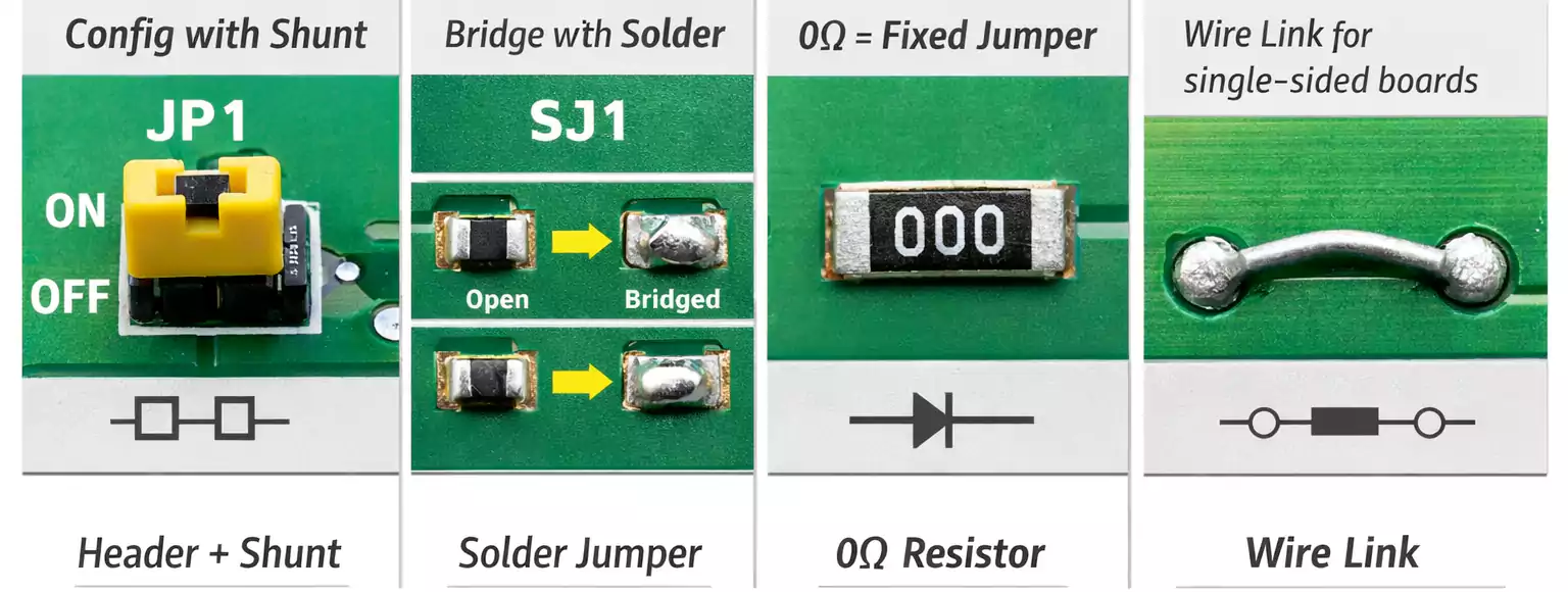
1. Header + Shunt Jumpers
The classic two-pin header with a removable cap (shunt).
Used to enable or disable features, select voltage, or set firmware options.
Example: JP1 = USB Power Source Selector.
2. Solder Jumpers (SJ)
Two or three small pads bridged by solder.
Designers use them to make permanent or reconfigurable connections on compact boards.
Open = disconnected; closed = shorted.
3. 0-Ohm Resistors
SMD parts marked “0” or “000” that act as fixed jumpers—reflow-soldered and reliable.
They simplify automated assembly while serving as electrical links.
4. Wire Links (LK)
A simple piece of insulated wire bridging two points, common on single-sided PCBs, where routing space is limited.
Using ECAD Tools or the BOM to Confirm Parts
When documentation is available, PCB Components Identification becomes easy:
- Open tOpen the schematic or layout in your ECAD tool (Altium, KiCad, OrCAD, etc.). Search the reference designator (e.g., U7) to locate it on both the schematic and layout. Then look up the Bill of Materials (BOM) for the manufacturer part number, value, and package.
- Verify with the datasheet: look for package outline, pin-1 location, and polarity.
No documentation? Measure package dimensions, observe its location in the circuit (power, logic, RF section), and use visual search to find matches by shape and marking.
Quick Testing & Troubleshooting
Even if you can identify parts visually, confirming their health ensures you’ve correctly identified them.
- Visual inspection: Burn marks, cracked housings, or bulging electrolytic capacitors often mean failure.
- Continuity & resistance: Use a multimeter to check for open or shorted resistors, jumpers, and fuses.
- Diode test mode: Verify diode and transistor junctions. A typical forward drop is 0.6–0.7 V for silicon.
- Compare symmetry: In multi-channel circuits (e.g., left/right audio), identical components should measure similarly.
- Thermal check: A part that heats up abnormally during operation may be defective.
Always discharge capacitors and use ESD protection when probing a live board.
Reading Markings & Polarity
1. Resistor Codes
SMD resistors use three- or four-digit numbers:
- 472 = 4.7 kΩ (47 × 10²)
- 1001 = 1 kΩ (100 × 10¹)
Color-band resistors use four or five rings; use a color code chart to decode.
2. Capacitor Codes
Electrolytic capacitors show capacitance + voltage (e.g., 10 µF 16 V).
Tantalum capacitors have a “+” sign near the positive lead.
Ceramic SMD capacitors may be unmarked—value is usually found from the BOM.
3. IC & Transistor Markings
The top surface code or short number identifies the device family.
Pin 1 is marked by a dot, notch, or beveled corner.
For dual-row ICs, pin numbers increase counterclockwise around the package.
4. Magnetic & Filter Components
Ferrite beads or common-mode chokes often bear “FB” or no code at all.
Their function is inferred by placement—usually on power or signal input lines.
Frequently Asked Questions
How do I identify PCB components quickly?
Follow the 3-step method: find the silkscreen code, check shape and markings, and verify with a multimeter.
What is a PCB jumper, and how is it labeled?
A small short-circuit connection labeled JP, SJ, or LK is used for configuration or routing.
How can I find pin 1 on an IC?
Look for a notch, dot, or beveled corner on the package—this marks pin 1.
Can a solder bridge be intentional?
Yes. That’s called a solder jumper. Designers use them for optional connections or version control.
What tools are most useful for PCB identification?
A multimeter, magnifying glass or microscope, ESD wrist strap, tweezers, and good lighting.
Final Thoughts
PCB Components Identification doesn’t require years of engineering experience—just practice and observation.
Start with the basics: read the reference designators, note shape and polarity, verify in software or BOM, and test with a multimeter.
With time, you’ll be able to look at any circuit board and instantly understand its structure and function.
PCB jumpers, markings, and reference codes are the language that every circuit “speaks.” Once you learn to read it, you can repair, reverse-engineer, or design with confidence.
