


Printed circuit boards (PCBs) are the heart of most modern electronic products. As devices get smaller and faster, designers push for tighter wiring, smaller vias, and more layers. High-Density Interconnect (HDI) PCBs are one of the key technologies that enable this. HDI boards use very small holes and advanced stacking to connect layers with minimal space. Laser drilling, especially with CO₂ lasers, is one of the key tools that let manufacturers make these ultra-small holes.
In this article, we explain what PCB CO₂ laser drilling is, how it works, its strengths and limits, and how it compares to mechanical drilling. We also look at how laser drilling fits into the HDI PCB process.
What Is Laser Drilling in PCB Manufacturing?
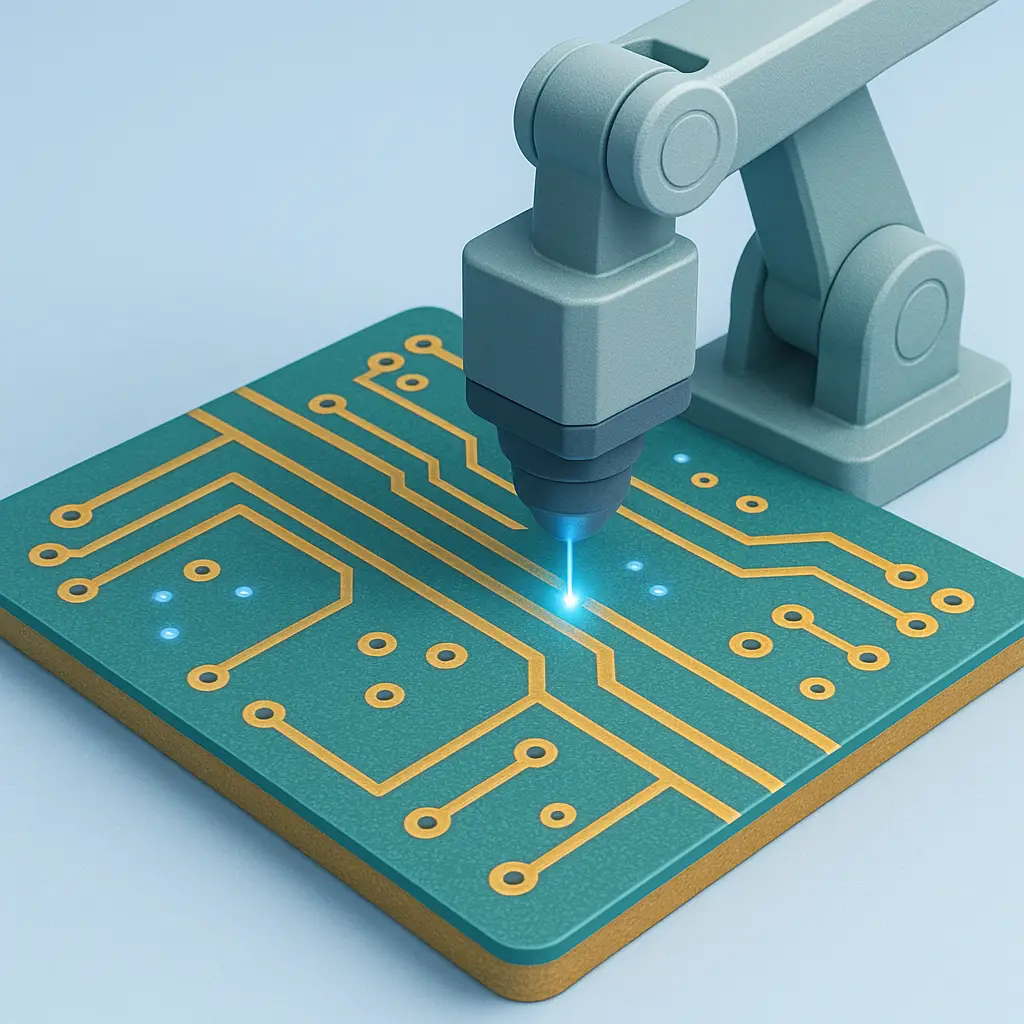
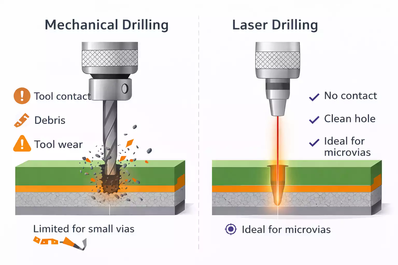
Laser drilling is a method that uses a focused light beam to remove material and make tiny holes in PCBs. Instead of a drill bit cutting into the board, a laser beam heats and vaporises material to create a hole. This is a non-contact process, meaning the material is removed without physical force.
There are two main types of lasers used in PCB drilling:
- CO₂ lasers – These operate in the far-infrared spectrum and work well on organic materials like FR-4 and polyimide.
- UV lasers – These operate at a much shorter wavelength and are better at drilling very tiny holes, and can remove copper as well as the dielectric.
This article focuses on CO₂ laser drilling, which excels at drilling holes in the dielectric layers that separate copper layers in a PCB.
How CO₂ Laser Drilling Works
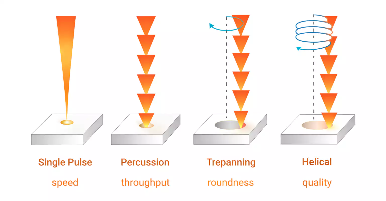
CO₂ lasers emit infrared light at a wavelength that organic materials absorb well. When the laser hits the board, the material quickly heats and vaporises. The beam can be focused to a very small spot, allowing fine holes to be drilled without mechanical stress.
The most common hole type on HDI boards is the microvia—tiny holes that connect just a few layers. A properly set CO₂ laser can drill these holes with good precision and repeatability.
One key idea is that CO₂ lasers interact differently with different materials. Organic PCB substrates, such as FR-4, absorb laser energy and vaporise cleanly. Copper reflects much of that light, so the laser tends to “stop” when it hits a copper layer. This natural stopping effect helps create controlled blind vias that terminate at the next copper layer.
What CO₂ Laser Drilling Can Do
CO₂ laser drilling brings several important benefits in PCB production:
1. Tiny Hole Sizes
Laser drilling can create holes much smaller than those that mechanical drills can. Mechanical drilling tools can struggle below 0.15 mm (150 μm), whereas laser drilling is routinely used for smaller hole diameters typical of microvias.
This makes laser drilling ideal for high-density boards with lots of fine routing. Microvias allow signals to pass between layers without using larger through-holes that consume more space.
2. High Precision and Clean Holes
Because the laser beam can be precisely controlled, the repeatability of hole position and size is high. The laser’s non-contact nature means there is no tool wear or vibration, which helps keep holes consistent.
3. Works on Many Materials
CO₂ lasers can process a wide range of PCB materials, including FR-4, polyimide, and flexible substrates. Because they do not physically touch the board, they do not cause mechanical stress or cracking that a drill bit might.
4. Good Throughput
For boards with many microvias, laser drilling can be faster than mechanical drilling, especially when hole counts are very high. This helps reduce cycle time for complex HDI boards.
Limits of CO₂ Laser Drilling
Like all manufacturing methods, CO₂ laser drilling has limits.
1. Hole Size Floor
CO₂ lasers are great for holes down to about 0.1–0.15 mm (100–150 μm), but below that, they become less effective. For extremely small holes (e.g., 50–80 μm or less), other lasers, such as UV lasers, are usually used because they can drill through both copper and dielectric materials with less heat.
2. Copper Interaction
CO₂ lasers are not very efficient at removing copper because copper reflects most of the infrared energy. This is why CO₂ lasers are mostly used for dielectric drilling. When copper must be removed first (such as for through-holes or deeper drilling), other lasers or pre-etch steps might be used.
3. Depth Control
Controlling how deep the laser drills can be harder without a metal stop layer. Without a stop layer, depth variations and tapering (a hole that is wider at one end than the other) can occur if the depth-to-width ratio is large.
4. Cost
Laser drilling machines, especially those designed for high-precision PCB work, are expensive. This means a higher capital cost compared to mechanical drills. However, for high-density boards, the benefits often outweigh the expense.
Mechanical Drilling vs. CO₂ Laser Drilling
It’s useful to compare the two main drilling methods in PCB manufacturing:
Mechanical Drilling
Mechanical drilling uses a rotating bit to cut holes. This method works well for larger holes and through-holes, and is cost-effective for boards with standard hole sizes.
However, mechanical drills have limits. They wear out over time, break on thin or fragile boards, and struggle with very small holes because the drill bits are fragile and slow at those sizes. Mechanical drilling also introduces vibration and stress into the board.
CO₂ Laser Drilling
Laser drilling removes material with a laser rather than a cutting tool. This avoids wear and tear and keeps tiny holes cleaner. It also works better on thin, delicate areas without damaging nearby structures or causing delamination.
Laser drilling does not replace mechanical drilling for all hole types. For standard through-holes or larger holes (above 0.15 mm), mechanical drilling remains common and is often more cost-effective.
Manufacturers use lasers for microvias and small holes, while mechanical drills handle larger holes.
Why Laser Drilling Matters for HDI PCBs
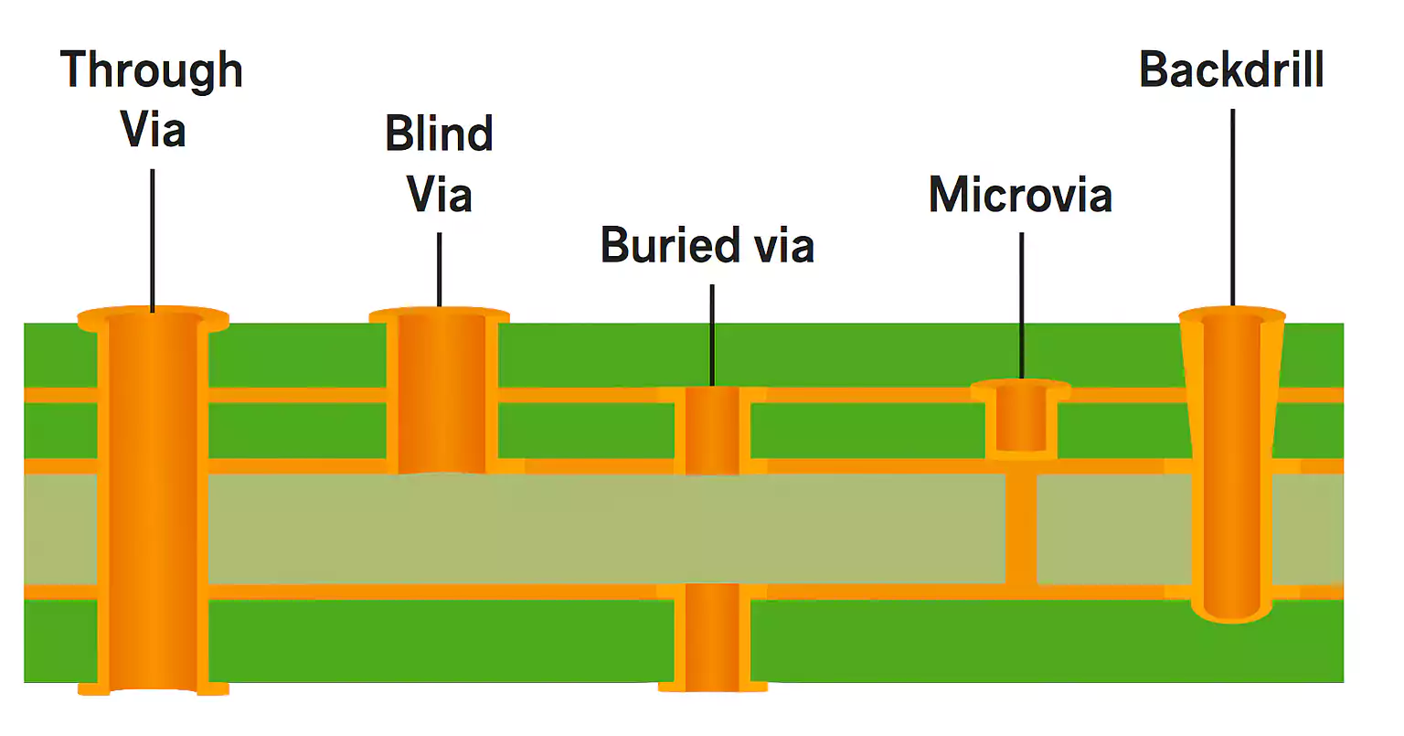
High Density Interconnect (HDI) PCBs are boards with very high wiring density. They pack many connections into a small area. These boards often use:
- Microvias (very small vias)
- Blind and buried vias (vias that don’t go through the whole board)
- Stacked vias
- Sequential lamination (building layers step by step)
Laser drilling creates the microvias needed for HDI, enabling stacked, connected layers with minimal space. Without laser drilling, making reliable microvias for HDI boards would be much harder and slower.
HDI boards enable modern designs such as smartphones, tablets, and high-speed data equipment. They enable routing signals in tight spaces without running out of room.
Typical Process in Laser Drilled PCB Manufacturing
Here’s how CO₂ laser drilling fits into a PCB manufacturing flow for HDI boards:
- Layer Stack and Copper Patterning – Inner copper layers are etched and prepared.
- Laser Drilling – The CO₂ laser drills holes in the dielectric until the next copper layer.
- Debris Removal – Material left in the hole is cleared so plating can stick.
- Copper Plating – Holes are plated with copper to make electrical connections.
- Lamination – The board is pressed and heated with prepreg layers to bond.
- Repeat for HDI Layers – For multi-HDI layers, drilling and plating repeat in sequence.
Laser drilling is usually automated and integrated into modern PCB lines for speed and repeatability.
Quality and Reliability Considerations
The quality of drilled holes affects board reliability. Key things manufacturers check include:
- Hole cleanliness and shape – Clean walls and minimal taper help ensure good plating.
- Aspect ratio – The ratio of depth to diameter should not be too high, or plating may be uneven.
- Material residue – Leftover material can interfere with copper plating and cause failures.
Good process control and inspection steps help ensure laser-drilled vias meet quality standards.
Summary: When to Use CO₂ Laser Drilling
Laser drilling, especially with CO₂ lasers, is an essential technology for modern PCB production. It enables:
- Small microvias for HDI designs
- Precise hole placement with less damage
- Higher throughput for dense boards
For designers and engineers working on advanced PCBs, understanding how CO₂ laser drilling works and where it fits best can help ensure reliable, manufacturable boards with excellent performance.
