


When you hand someone a business card that lights up, links to your portfolio, or literally is a functioning circuit board, you’ll never be forgotten.
PCB business card is the ultimate fusion of engineering skill and personal branding. Whether you’re a hobbyist, engineer, or maker, a PCB card transforms first impressions into conversation starters.
This guide walks you through everything from what a PCB business card is and how NFC works, to board design choices, costs, and troubleshooting.
What Is a PCB Business Card and Why It Stands Out
A PCB business card replaces paper with copper, solder mask, and creativity. It’s a real printed circuit board that functions as your personal brand’s handshake — but with circuitry.
There are three main styles:
- Visual or artistic cards — emphasize design, copper pattern, or etched logos.
- Functional or tool cards — include measurement grids, component outlines, or pinout references, inspired by Salvaged Circuitry’s “tool card” concept.
- Interactive or electronic cards — embed NFC chips, LEDs, or USB connections, letting recipients scan, light up, or even play with your design.
These appear at hackathons, tech fairs, job interviews, and as creative giveaways. They cost more than paper cards but offer unmatched memorability and interactivity.
Two Core Routes: NFC vs. Non-NFC (How to Choose)
The biggest design fork comes early:
Do you want a touch-activated interactive card or a simple, always-useful PCB tool?
Route A – NFC Interactive Card
Tap the card on a phone, and it instantly opens your website, LinkedIn, or portfolio.
NFC cards use small chips like NT3H1101 or NT3H1201 from NXP that communicate with smartphones via the 13.56 MHz NFC frequency.
You can program them using Android or specialized writer apps. Always use NDEF format to ensure compatibility with both Android and iOS.
And since iPhones read NFC only from the top edge, always back up your link with a visible QR code.
Route B – Non-NFC “Tool Card”
Not every card needs to be smart. Some makers design tool-style PCB cards with resistor codes, package footprints, trace-width charts, or millimeter scales printed right on them.
They’re always readable, require no power, and double as reference rulers.
They appeal to those who value practical engineering aesthetics and eliminate concerns about NFC compatibility.
NFC Design Fundamentals (and the Mistakes to Avoid)
If you go the NFC route, here’s what really matters.
Chip and Tag Selection
The NT3H1101 and NT3H1201 from NXP differ mainly in memory size and programmability. The 1201 supports I²C for updates.
Other brands exist, but ensure they support NDEF records for universal smartphone recognition. Avoid MIFARE Classic unless you need encrypted access — it’s not ideal for contact sharing.
Antenna and Resonance Tuning
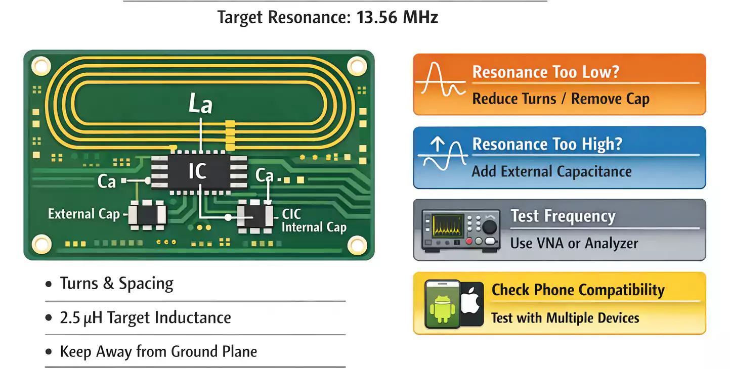
NFC communication relies on inductive coupling — your card’s loop antenna creates a magnetic field that couples with the phone’s NFC coil.
- The target frequency is 13.56 MHz.
- The antenna behaves as an inductor (La) that, together with the chip’s internal capacitance (CIC) and any external tuning capacitor (Ca), forms a resonant LC circuit.
- Your goal: achieve resonance near 13.56 MHz.
Begin with ~2.5 µH inductance and adjust the number of turns, trace width, and spacing. Instructables’ tutorials provide examples of loop layout and testing.
Testing and Fine-Tuning
Use a VNA (Vector Network Analyzer) or impedance analyzer to check the resonant peak.
If the resonance shifts too low, reduce the inductance (fewer turns).
If too high, add a small parallel capacitance.
Keep metals and ground planes away — even a logo’s copper pour can detune the antenna.
Always test the card with multiple phones and cases, since iPhones have smaller NFC sweet spots.
Energy Harvesting Tricks
Some NFC chips can harvest energy from the RF field—enough to blink an LED when a phone is nearby. This “no-battery demo” effect, seen in Tindie’s customizable NFC card, adds instant wow-factor without extra complexity.
Designing a Non-NFC or “Tool” PCB Card
Tool-style PCB cards focus on utility and legibility.
Take inspiration from Salvaged Circuitry’s PCB business card, which doubles as a reference ruler.
Design Tips
- Include IC footprints, SMD pad sizes, and resistor/capacitor scales.
- Add a trace-width vs. current table or via size chart.
- For visual clarity, use contrasting solder mask and silkscreen colors — black mask with white silkscreen or white mask with black text.
- ENIG (gold finish) offers a premium look and greater durability than HASL. These mini-tools keep your brand visible far longer than ordinary paper cards.d.
Engineering Choices: What the Pros Get Right
Designing for function and feel involves trade-offs between cost, manufacturability, and usability.
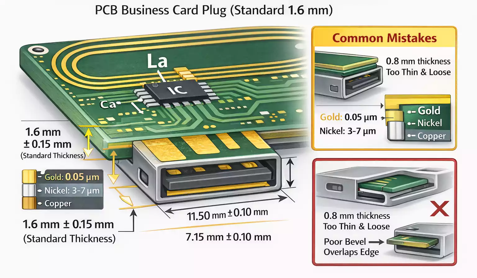
Thickness and Hand Feel
- 0.6 mm boards: Thin, flexible, and wallet-friendly (common for NFC cards).
- 1.6 mm boards: Rigid, tactile, and suitable for USB-A edge connectors.
If you plan a USB plug demo, stick with 1.6 mm — thinner boards can wobble or lose contact.
Surface Finish
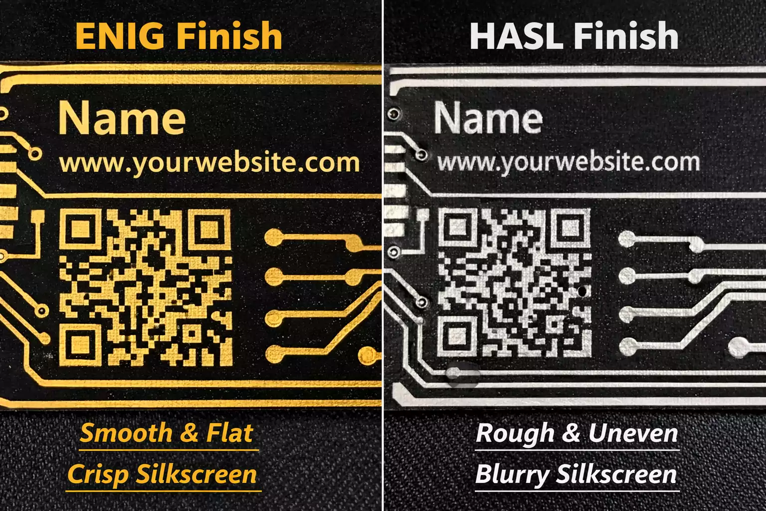
- ENIG (Electroless Nickel Immersion Gold): smooth, corrosion-resistant, excellent contrast for silkscreen and QR codes.
- HASL (Hot Air Solder Leveling): cheaper but less flat — can distort text or QR readability.
LEDs and Display Tricks
For cards with multiple LEDs, engineers often use Charlieplexing to control up to n × (n – 1) LEDs with n microcontroller pins.
It saves IO pins but requires careful timing and refresh cycles to maintain brightness consistency.
Marian’s blog detailed how Charlieplexing enabled compact LED animations without adding chips.
USB-A Edge Contacts
Some cards double as plug-in devices. The USB-A edge must match the connector’s mechanical tolerance:
1.6 mm thickness ±0.15 mm, beveled at 45°.
Use ENIG plating for wear resistance and, if necessary, a thin solder “bump” to improve contact.
From Concept to Finished Card: Step-by-Step
A PCB business card project follows the same flow as any small electronic design.
Step 1 – Define the Goal
Do you want to impress, teach, or demonstrate?
A flashy NFC card for events differs from a durable tool card for everyday use.
Set your constraints — functionality, time, and budget.
Step 2 – Schematic and Layout
For NFC: reserve a clean area for the coil and keep it clear of ground planes.
For LEDs or USB, plan current paths and avoid overlapping copper that could detune the antenna.
Include:
- Your name, title, and contact URL
- A small QR code backup
- Readable silkscreen (minimum font height ~0.8 mm)
Step 3 – Fabrication Rules
Follow your manufacturer’s DFM rules:
- Minimum trace width: 4–6 mil
- Via size: ≥ 0.3 mm
- Solder mask clearance: 3 mil
- Rounded corners for pocket safety
Choose solder mask color and finish early — white mask looks sleek but gets dirty; black hides fingerprints but can reduce contrast.
Step 4 – Assembly & Programming
For NFC chips or microcontrollers:
- Use solder paste and hot-air or reflow.
- Clean flux residues thoroughly.
- Program NFC memory via smartphone app (e.g., NXP TagWriter).
Test on both Android and iPhone. Store URLs, vCards, or contact files in NDEF format.
Step 5 – Testing
Check:
- Read distance with multiple phone models.
- LED brightness and pattern consistency
- QR code readability under normal lighting
- Durability: pocket friction, scratches, and bending.
Design Inspiration and Future Trends
The creativity in PCB business cards keeps evolving, as seen on Hackaday’s running feature series.
Here are some standout directions:
- NFC + LED Hybrid Cards — light up your logo when tapped.
- Game Cards — tiny Pong or Tetris animations on microcontrollers.
- Self-Booting Résumé — USB-A card that mounts as a drive and shows your CV or GitHub link.
- Functional Ruler Cards — measurement grids, pinout cheatsheets, or conversion charts.
- Dual-Color Masks — gold-on-black for luxury branding; clear mask for copper art.
Even large companies now commission small runs for tech conferences — not just for novelty, but for genuine brand differentiation.
Common Problems and How to Fix Them
Even experienced makers hit a few snags. Here’s how to avoid (or fix) them.
| NFC range too short | Coil not resonating at 13.56 MHz, metal interference, poor phone alignment | Adjust coil turns/capacitor; increase distance from copper pours; test with multiple phones |
| LEDs dim or flicker | Refresh rate too low, wrong pull-ups, insufficient current | Optimize Charlieplexing timing, use proper resistor values |
| USB-A not recognized | Thickness or bevel off, poor plating contact | Add solder bump or change finish to ENIG; verify 1.6 mm spec |
| Silkscreen blurred | Too small font, HASL unevenness | Use ENIG and ≥ 0.8 mm font height |
| QR code unreadable | Low contrast or reflection | High-contrast mask, matte finish, avoid curved surfaces |
Testing each variable one at a time saves headaches — especially with NFC detuning, where even tiny layout changes shift resonance.
Conclusion
A PCB business card isn’t just a gimmick — it’s a living example of your design philosophy.
It demonstrates attention to detail, technical competence, and creativity all in a 3.5″ × 2″ frame.
Your PCB card is more than contact info — it’s your personal prototype of innovation.
