

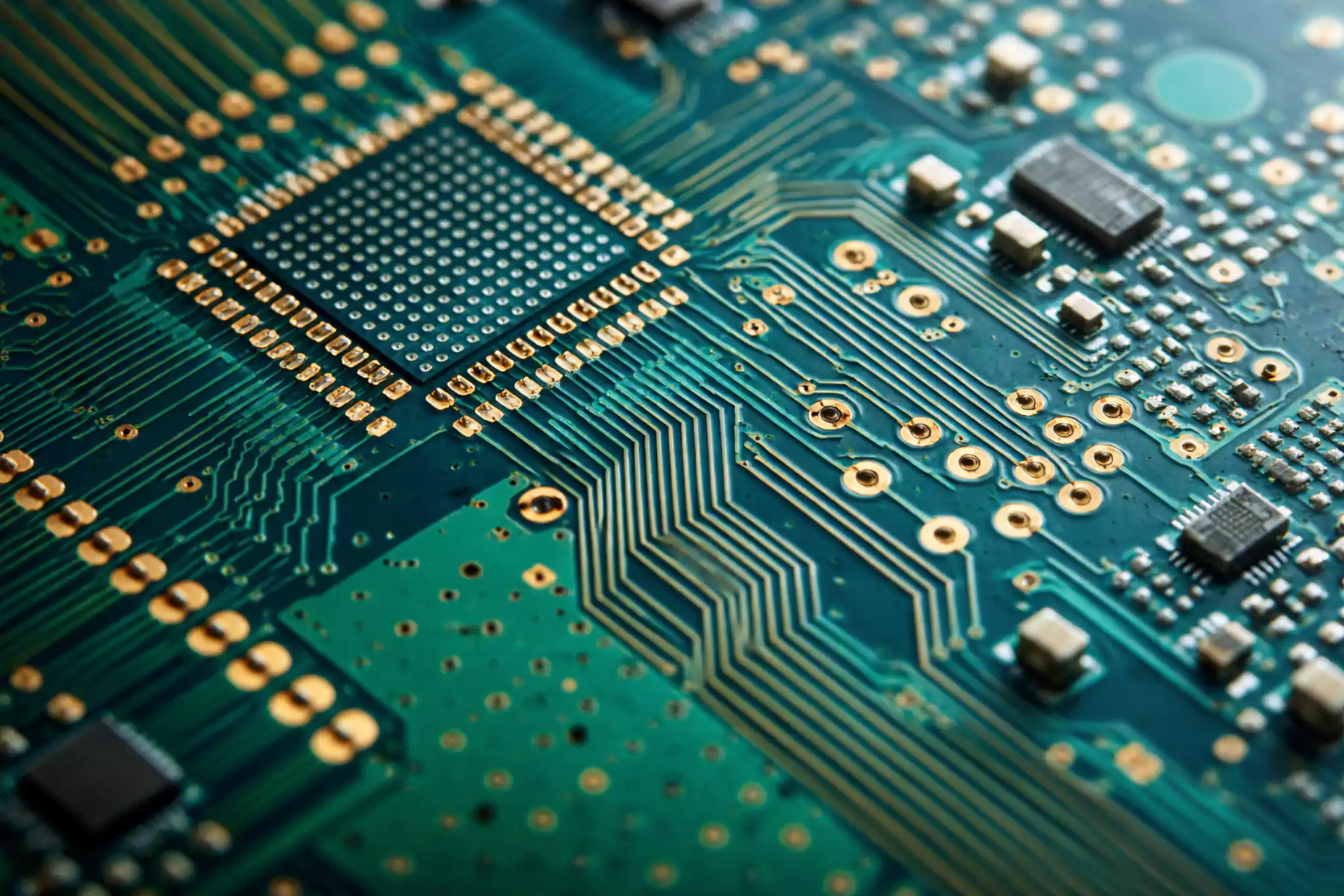

When every board on your production line carries hundreds of components and tight tolerances, PCB board testing is the last checkpoint between a working product and a costly failure.
Testing ensures correct assembly, soldering, and function—catching issues before customer delivery.
This guide explains the most common PCB testing methods, how to choose among them, and how to test a PCB step by step.
What Is PCB Board Testing?
In electronics manufacturing, PCB Board Testing verifies the electrical and functional performance of a printed circuit board, while inspection focuses on visual or structural defects.
- Inspection (AOI/AXI) detects missing or misaligned components, solder bridges, and voids using optical or X-ray imaging.
- Testing (ICT, Flying Probe, Functional) validates electrical behavior, continuity, resistance, shorts, and logic response.
Together, inspection and testing form the foundation of quality assurance, ensuring every PCB shipped can power on safely, communicate properly, and meet design intent.
Choosing the Right Testing Method
Different PCB Board Testing methods balance cost, coverage, and throughput. The optimal strategy depends on your production volume, design maturity, and reliability goals.
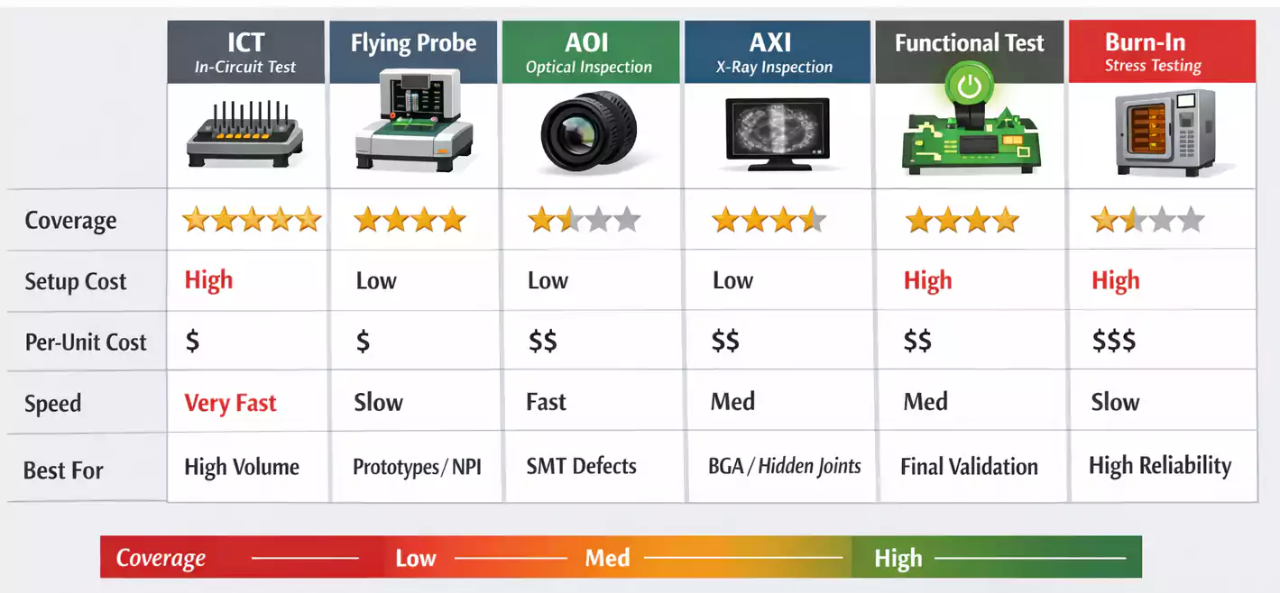
| In-Circuit Test (ICT) | Electrical | ★★★★★ | High | Very Fast | High-volume, stable designs |
| Flying Probe | Electrical | ★★★★☆ | Low | Slow | Prototypes, small batches |
| AOI | Optical | ★★★☆☆ | Medium | Fast | SMT defects & early inspection |
| AXI (X-Ray) | Optical | ★★★★☆ | High | Medium | BGA & hidden solder joints |
| Functional Test | Electrical | ★★★★★ | Medium | Medium | Final validation |
| Burn-In / Stress | Environmental | ★★★☆☆ | High | Slow | High-reliability sectors |
Core PCB Board Testing Methods Explained
1. In-Circuit Test (ICT)
ICT uses a bed-of-nails fixture to simultaneously make electrical contact with hundreds of test points on the board. It measures resistance and capacitance, checks diode polarity, and checks for shorts or opens.
Advantages:
- Fast and highly repeatable for volume production.
- Detects multiple defects simultaneously with high coverage.
Limitations:
- Expensive custom fixture and long setup time.
- Requires accessible test pads and a consistent board design.
ICT is ideal for high-volume, mature designs where throughput and coverage justify the investment in fixtures.
2. Flying Probe Test
Flying Probe testing uses a set of programmable needles that move across the board to sequentially contact test points—no fixture required.
Advantages:
- Zero fixture cost; easy to modify for new revisions.
- Great for prototypes, NPI (New Product Introduction), and low-volume builds.
Limitations:
- Slower than ICT (probes move mechanically).
- Lower parallel coverage, so longer cycle time.
Flying Probe offers flexibility and fast setup, ideal when rapid prototyping outweighs cycle time.
3. Automated Optical Inspection (AOI)
AOI systems use high-resolution cameras and algorithms to compare solder joints, component placement, and polarity against a golden reference image.
Advantages:
- Non-contact, fast, and ideal right after SMT reflow.
- Detects missing, reversed, or misaligned parts before electrical testing.
Limitations:
- Can’t verify electrical continuity or internal solder quality.
- May produce false positives that require manual review.
AOI best serves as a screening tool before ICT or functional testing.
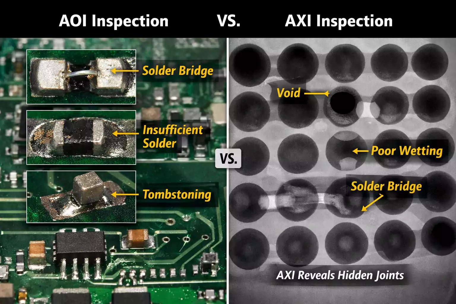
4. Automated X-Ray Inspection (AXI)
AXI uses 2D or 3D X-ray imaging to “see” hidden joints beneath BGAs, QFNs, or stacked packages.
Advantages:
- Reveals voids, cold solder joints, or bridging inside packages.
- Non-destructive and high precision.
Limitations:
- Expensive equipment; slower than AOI.
- Typically used for sample or critical inspection, not 100% production screening.
AXI complements AOI for complex assemblies needing non-visual inspection.
5. Functional Testing
Functional test (FCT) powers the board and verifies that the system behaves as designed—checking voltage rails, communication interfaces, firmware responses, and timing.
Advantages:
- Closest to real-world performance.
- Detects issues that lower-level electrical tests miss.
Limitations:
- Requires customized test software, fixtures, or harnesses.
- Development effort scales with product complexity.
Functional testing ensures a PCB works properly before integration into the final product.
6. Burn-In or Environmental Stress Testing
Burn-in exposes PCBs to elevated voltage, temperature, or load for hours or days to catch early failures (“infant mortality”).
Advantages:
- Filters weak components early in the life cycle.
- Standard practice for aerospace, medical, and automotive sectors.
Limitations:
- Time-consuming and may accelerate wear.
- Typically reserved for high-reliability applications.
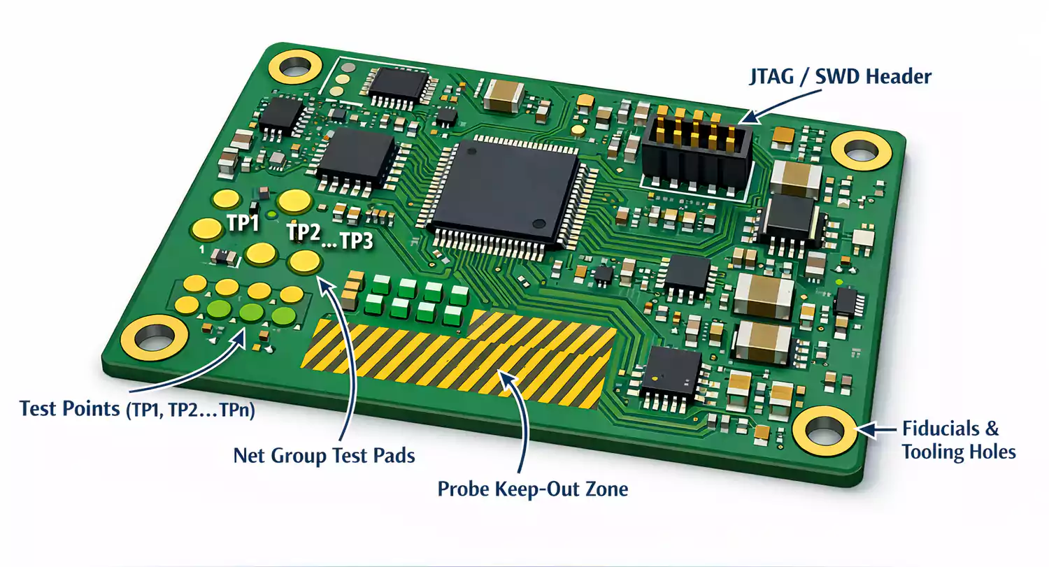
Design-for-Test (DFT): Catch Problems Before They Reach Production
Improve testing during PCB design—DFT saves time, reduces costs, and prevents rework.
Key DFT practices:
- Add dedicated test pads for each net or critical node—keep them probe-accessible.
- Maintain consistent pad size and spacing for bed-of-nails or flying probe access.
- Include boundary scan connectors (JTAG, SWD, UART) for programming and debugging.
- Document test requirements—tolerances, expected voltages, pass/fail criteria—in design files.
These small design investments pay off during the transition from prototype to production, enabling a seamless migration from Flying Probe to ICT testing.
How to Test a PCB Board: Step-by-Step Process
If you’re testing a single prototype or troubleshooting a board, follow this practical workflow.
Step 1: Visual Inspection (Unpowered)
Check for solder bridges, missing parts, reversed-polarity components, and poor joints using a magnifier or an AOI system. Verify silkscreen orientation and mechanical alignment.
Step 2: Continuity and Short Checks
Use a multimeter in continuity mode to ensure no short between power and ground, and that all key nets are connected.
Pay special attention to high-current traces, connectors, and power rails.
Step 3: Pre-Power Verification
With the board unpowered, measure the resistance between the rails to detect unexpected shorts.
Then apply low-current power and verify each voltage regulator output individually.
Step 4: Power-On Tests
Use a programmable power supply with current limit protection.
- Bring up each rail sequentially.
- Observe startup behavior with an oscilloscope—check ripple, switching frequency, and clock signals.
- Confirm reference voltages and I/O logic levels.
Step 5: Minimal Firmware / Boot Test
Load a minimal firmware or test script to confirm MCU boot, peripheral enumeration, and UART/USB communication.
This verifies not only power delivery but also system interconnects.
Step 6: Functional Validation
Exercise major interfaces—sensors, communication ports, actuators, and memory.
Measure output signals under load. Record pass/fail results in a log for traceability.
Step 7: Troubleshooting Common Issues
| Board draws too much current | Shorted rail, reversed diode | Remove suspect ICs, thermal camera |
| No clock or reset | Missing oscillator, wrong crystal load | Probe with oscilloscope |
| MCU not booting | Flash or power sequencing error | JTAG readout, firmware check |
| Intermittent faults | Cold solder, via crack | Gentle mechanical tap test |
FAQ: Common Questions About PCB Board Testing
1. Should I use Flying Probe or ICT?
Use a Flying Probe for prototypes or frequent design revisions—it’s flexible and inexpensive to get started.
Switch to ICT when the design stabilizes and production volume grows to reduce test time per unit.
2. Is AOI alone enough for quality control?
No. AOI only verifies visible defects. Combine it with electrical or functional tests for complete coverage.
3. Can I migrate from Flying Probe to ICT later?
Yes, if your board follows DFT rules—accessible test pads and stable layout. This is a common evolution path.
4. Who develops Functional Tests?
Usually, the OEM or engineering team defines the test criteria, while the EMS partner helps build fixtures, harnesses, and automation scripts.
Conclusion
PCB Board Testing isn’t a one-time task — it’s a strategy that grows with your product. By combining visual checks, electrical tests, and functional validation, you catch issues early and ship boards that perform as intended.
Design for testability from the start, choose the right methods for your scale, and work with a partner skilled in ICT, Flying Probe, and Functional Test. The result? Fewer failures, faster launches, and peace of mind at every stage.
